Clocks, Clocks –14 – Altera Transceiver Signal Integrity Development Kit, Stratix IV GX Edition User Manual
Page 24
2–14
Chapter 2: Board Components
Clocks
Transceiver Signal Integrity Development Kit,
November 2011
Altera Corporation
Stratix IV GX Edition Reference Manual
Clocks
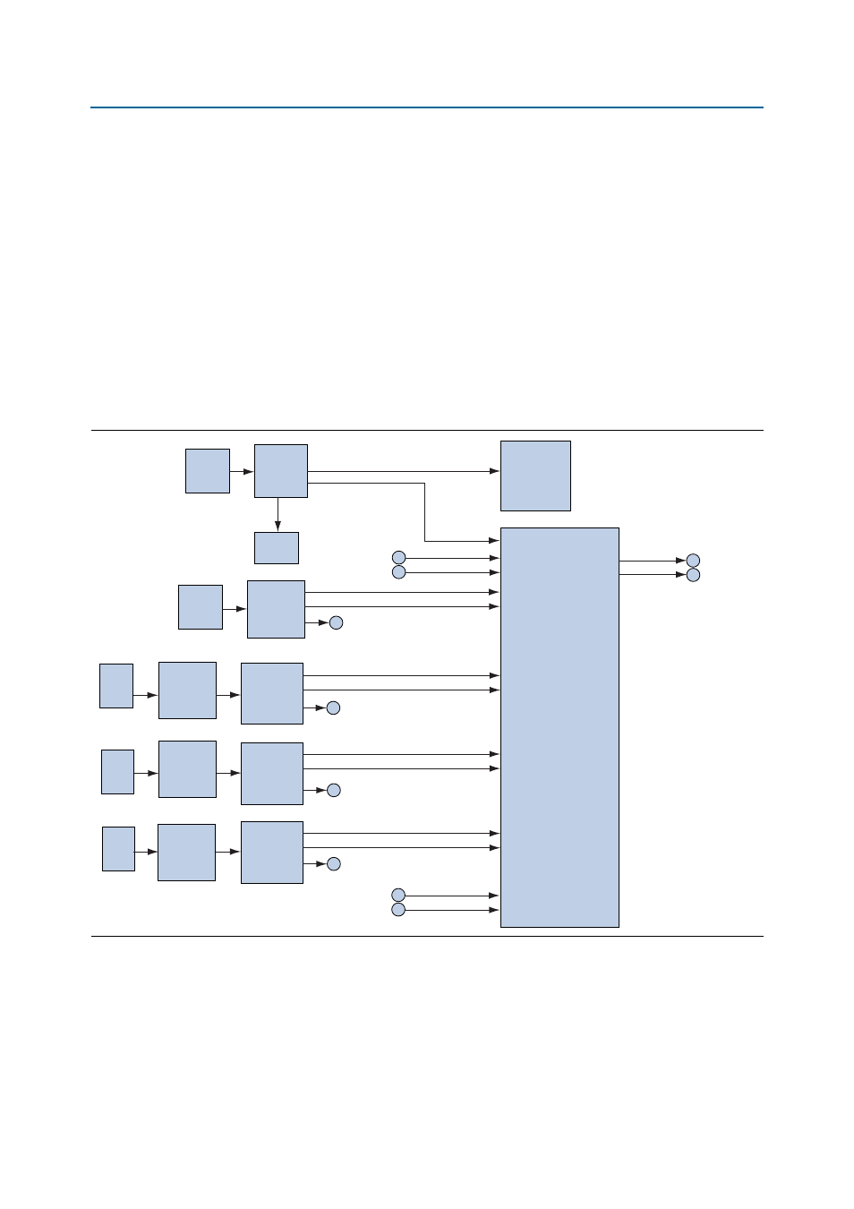
Clocking for the Stratix IV GX transceiver signal integrity board is provided
separately for both the FPGA core and transceivers. The core clocks include a
dedicated 50-MHz clock, a spread spectrum clock capable of producing either
25-MHz, 100-MHz, 125-MHz, or 200-MHz clock, and a pair of SMA connectors to
receive a differential external clock. The dedicated transceiver clocks include a
100-MHz, 156.25-MHz clock source, and a socket for accepting a 5×7-mm 6-pin
oscillator. This socket has the flexibility of providing any custom oscillator frequency
to the transceivers. Additionally, if an oscillator with the desired frequency is not
readily available, the transceivers can receive a differential clock from an external
source through a pair of SMA connectors.
shows the Stratix IV GX transceiver signal integrity development board
clocking diagram.
Figure 2–6. Stratix IV GX Transceiver Signal Integrity Board Clocking Diagram
50-MHz
OSC (Y2)
ICS8304
CLKBUF
(U20)
MAX II CPLD
(U32)
CLKIN SMA
(J14, J15)
Trigger
SMA (J18)
Trigger
SMA (J21)
25-MHz
XTAL (Y2)
Trigger
SMA (J22)
Trigger
SMA (J23)
CLKIN SMA
(J19, J20)
ICS557
Spread
Spectrum
CLKBUF
(U21)
DIPSW
(SW2)
Stratix IV GX
FPGA
(U33)
CLKOUT SMA
(J16, J17)
OSC
Socket
(Y3)
ICS8543
CLKBUF
(U22)
EN JMP
(J66)
100 MHz
OSC
(Y4)
ICS85411
CLKBUF
(U23)
ICS85411
CLKBUF
(U24)
EN JMP
(J67)
156.25 OSC
(Y5)
EN JMP
(J65)