Altera Arria GX Development Board User Manual
Page 36
2–26
Reference Manual
Altera Corporation
Arria GX Development Board
October 2007
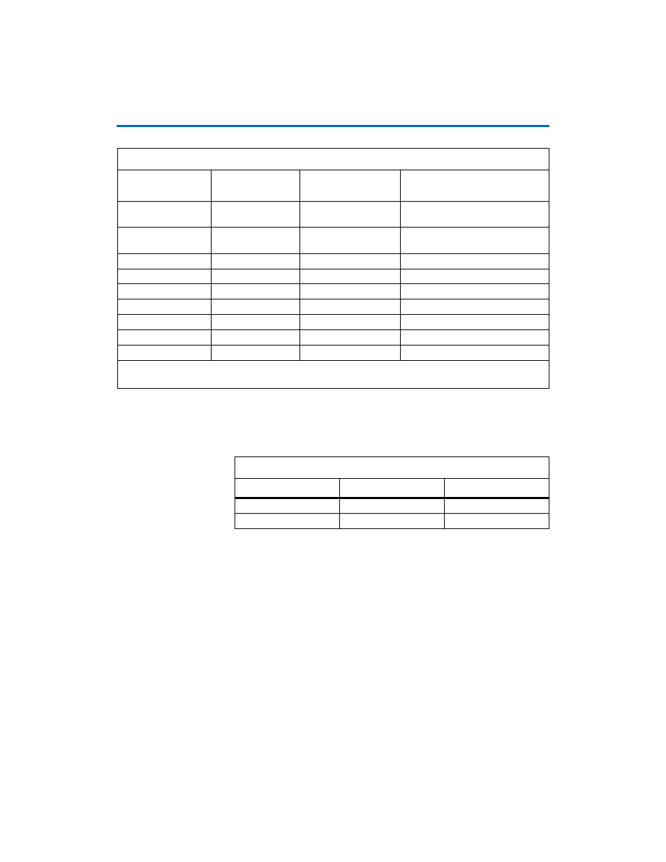
Standard Communication Ports
shows the minimum power levels that the Arria GX
development board guarantees from on-board power supplies. The
power rails are delivered via designated pins on the HSMC interface.
The Arria GX development board uses a Samtec connect to interface to
HSMC daughter boards.
shows the Samtec ASP-122952-01
used on the Arria GX development board. The socket is placed in the
“minimum keep-out board-edge layout” style.
Management serial
data line
2.5 V LVCMOS in/out
HSMA_SDA
A20
Management serial
clock line
2.5 V LVCMOS out
HSMA_SCL
A18
JTAG clock
N/A (part of chain)
JTAG_TCK
V17
JTAG mode select
N/A (part of chain)
JTAG_TMS
W19
JTAG data out
N/A (part of chain)
HSMA_JTAG_TDO
V19
JTAG data in
N/A (part of chain)
JTAG_TDI
N/A
Power
12 V
12V
N/A
Power
3.3 V
3.3V
N/A
Ground
Ground
GND
N/A
Note to
Table 2–24
:
(1)
When the MAX II device is bypassed, the HSMA_JTAG_TDO signal is connected to Arria GX device pin V19
.
Table 2–24. HSMC Interface Pin-Out (Part 2 of 2)
Description
Type
Schematic
Signal Name
Arria GX Device
Pin Number
Table 2–25. Minimum Guaranteed Power Levels
Voltage
Current Rating
MAX Wattage
12 V
1.0 A
12.0 W
3.3 V
2.0 A
6.6 W