Max ii cpld configuration controller, Max ii cpld configuration controller -13 – Altera Arria GX Development Board User Manual
Page 23
Altera Corporation
Reference Manual
2–13
October 2007
Arria GX Development Board
Board Components
lists the flash memory component reference and manufacturing
information.
MAX II CPLD Configuration Controller
The MAX II CPLD is primarily used for FPGA configuration and flash
programming. The target MAX II device is an EPM570 in a 100 ball FBGA.
The PFL megafunction is the basis for the MAX II CPLD design.
The MAX II CPLD is part of the board’s JTAG chain and can be
programmed using the Quartus II Programmer and a USB-Blaster cable.
The same JTAG interface is also used to program flash images.
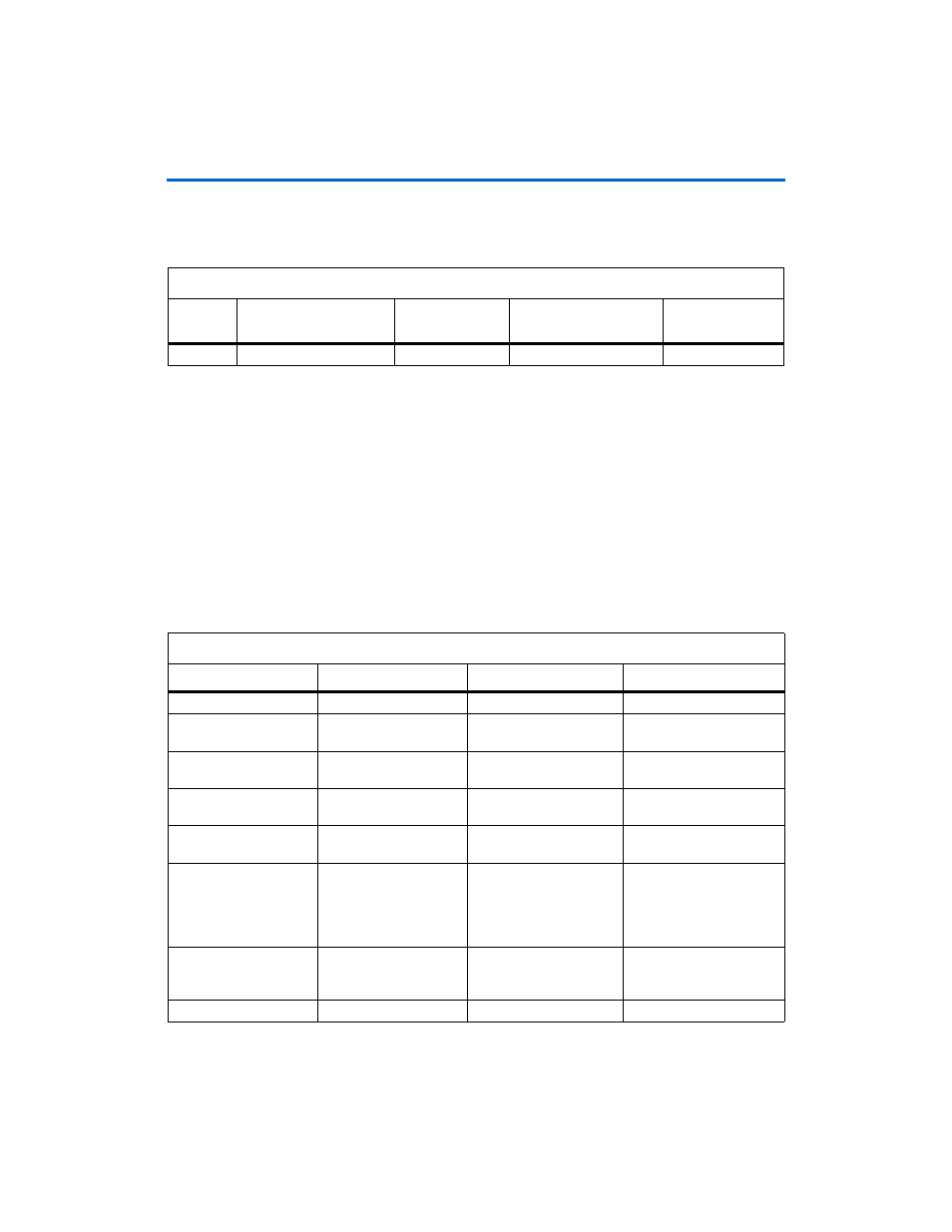
Table 2–10
lists the required MAX II CPLD signals and the corresponding
PFL megafunction design I/O requirements. Signal directions are relative
to the MAX II CPLD as far as direction and signaling standard.
Table 2–9. Flash Memory Component Reference and Manufacturing Information
Board
Reference
Description
Manufacturer
Manufacturer Part
Number
Manufacturer
Website
U6
Flash memory
Spansion
S29GL512N
www.spansion.com
Table 2–10. MAX II CPLD Signals & I/O Requirements (Part 1 of 2)
MAX II Pin Numbers
Schematic Signal Name
Description
Signal Type
C9
FPGA_CONFIG_DCLK
Configuration clock
3.3-V CMOS out
A7,A6,B6,A5,B5,A4,
B4,C4
FPGA_CONFIG_D(7:0)
Configuration data bus
3.3-V CMOS out
D8
CONF_DONE
FPGA
CONF_DONE
pin
connection
3.3-V CMOS in
D9
CONFIGn
FPGA
nCONFIG
pin
connection
3.3-V CMOS out
B10
STATUSn
FPGA
nSTATUS
pin
connection
3.3-V CMOS in
K2,K3,H4,J4,K4,
J5,K5,K6,J6,K7,K8,
H7,J8,H8,K10,J9,
H9,J10,H10,G8,G9,
G10,F10,F9
FLASH_A(24:0)
Flash address bus
3.3-V CMOS out
C2,B1,C1,D3,D2,
D1,E3,F2,F3,F1,
G1,H1,G2,G3,K1,J3
FLASH_D
(15:0)
Flash data bus
3.3-V CMOS in/out
F2
FLASH_CEn
Flash chip enable
3.3-V CMOS out