Altera Arria GX Development Board User Manual
Page 13
Altera Corporation
Reference Manual
2–3
October 2007
Arria GX Development Board
Board Components
Table 2–1
describes the components and lists their corresponding board
references.
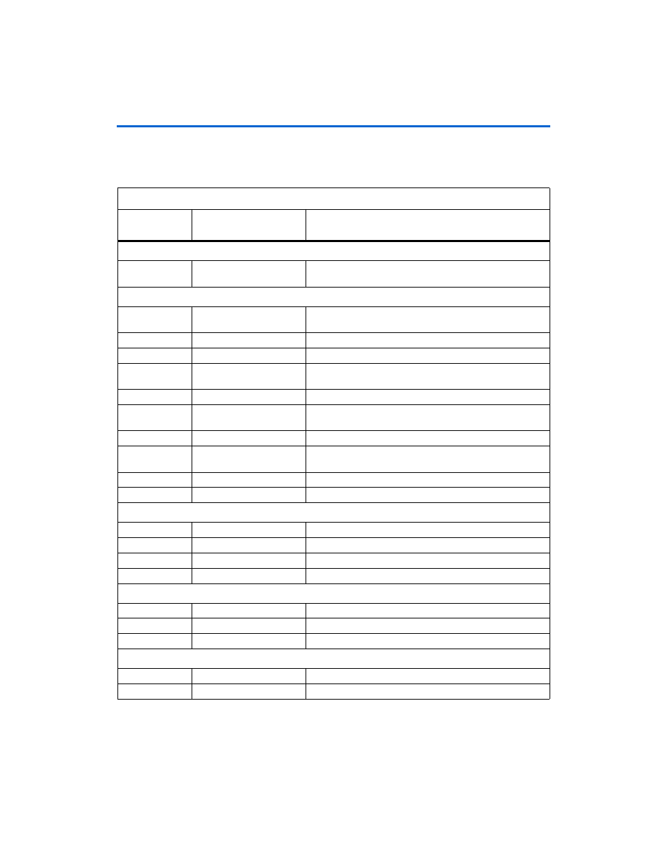
Table 2–1. Board Components & Interfaces (Part 1 of 2)
Board
Reference
Name
Description
Featured Device
U7
Arria GX FPGA
EP1AGX60D FPGA in a 780-pin flip-chip FineLine BGA®
(FBGA) package.
Configuration Status and Setup Elements
S6
Board configuration
DIP switch
DIP switch that controls the FPGA and MAX II device
configuration settings.
D19 and D20
PCIe mode LEDs
Yellow LEDs that display PCIe x1 or x4 mode.
D2
Configuration done LED
Green LED that displays configuration status.
D12 and D13
Channel activity LEDs
Yellow LEDs that indicate the RX and TX activity on HSMC
Port A.
D11
Power LED
Blue LED indicates when power is applied to the board.
D21, D22, D23
Voltage present LEDs
Green LEDs that indicate the presence of 1.5 V, 2.5 V, and
1.2 V power.
S5
Configuration push button
Push button to reconfigure the Arria GX device.
SW2, SW3
JTAG chain bypass
switches
Switches to include or exclude HSMC Port A and MAX II from
the JTAG chain.
D1
HSMC present LED
Green LED indicates when an HSMC card is connected.
J6
JTAG header
10-pin header for JTAG-based FPGA communication.
Clocks
X1
100 MHz
100-MHz oscillator
X2
125 MHz
125-MHz oscillator
X3
62.5 MHz
62.5-MHz oscillator
J4
SMA clock input
SMA connector that allows the provision of an external clock.
General User Input/Output
S1, S2, S4
User push-button switches
User-defined push-button switches.
D3-D10
User LEDs
Eight user-defined LEDs.
S3
User DIP switch
User-defined DIP switches.
Memory Devices
U8
DDR2 SDRAM
32 M x16 of DDR2 SDRAM
U6
Flash
512 Mbits of flash memory