Temperature sense, Temperature sense –60 – Altera DSP Development Kit, Stratix V Edition User Manual
Page 68
2–60
Chapter 2: Board Components
Temperature Sense
DSP Development Kit, Stratix V Edition
July 2012
Altera Corporation
Reference Manual
lists the power measurement ADC component references and
manufacturing information.
Temperature Sense
Temperature monitoring for the Stratix V GS die is achieved with a MAX1619
temperature sense device. The MAX1619 device connects to the MAX V CPLD
EPM2210 System Controller and the Stratix V GS device by a 2-wire SMB interface.
The MAX1619 device is located at address 0x1. This bus is also routed to a single
voltage and power monitor chip for the 12-V power rail at address 0x2.
The OVERTEMPn and TSENSE_ALERTn signals are driven by the MAX1619 temperature
sense device based on a programmable threshold temperature. The OVERTEMPn signal
is driven to the MAX V System Controller, which controls the OVERTEMPn signal. The
MAX V System Controller can control fan speed is based on a register setting and can
also override the MAX1619 device. For more information on this control, refer to the
MAX V System Controller source code found in the development board installation
directory
f
For more information on the development board installation directory, refer to the
The remote sense routes to the FPGA diode pins to measure the voltage drop. For
very accurate temperature readings, the I/O adjacent to the FPGA diode sense pins
must be halted.
5
S5_VCC_1p5
1.5
VCCD_FPLL
PLL digital power
VCCH_GXB
XCVR block level transmit buffers
VCCPT
Programmable power tech auxiliary
6
S5_VCCIO_2.5V
2.5
VCCIO_3A
I/O supply bank 3A
VCCIO_3B
I/O supply bank 3B
VCCIO_4B
I/O supply bank 4B (HSMC Port A)
VCCIO_7B
I/O supply bank 7B (HSMC Port A)
7
S5_VCCIO_1.5V
1.5
VCCIO_8A
I/O supply bank 8A (DDR3 RZQ)
VCCIO_8B
I/O supply bank 8B (DDR3)
VCCIO_8C
I/O supply bank 8C (DDR3)
VCCIO_8D
I/O supply bank 8D (DDR3)
8
S5_VCCA_GXB
3.3
VCCA_GXB
XCVR TX driver, RX receiver, CDR
Table 2–59. Power Rail Measurements Based on the GUI Selection (Part 2 of 2)
Number
Schematic Signal Name
Voltage (V)
Device Pin
Description
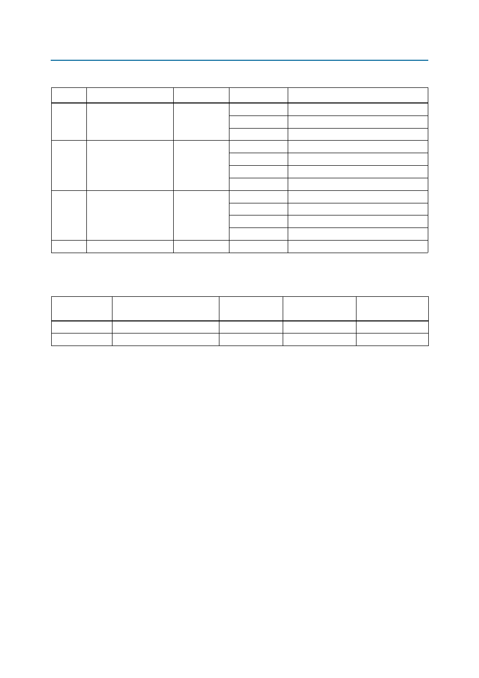
Table 2–60. Power Measurement ADC Component References and Manufacturing Information
Board Reference
Description
Manufacturer
Manufacturing
Part Number
Manufacturer
Website
U52
8-channel differential 24-bit ADC
Linear Technology
LTC2418CGN#PBF
U1
1-channel differential 14-bit ADC
Linear Technology
LTC2990IMS#PBF