Altera DSP Development Kit, Stratix V Edition User Manual
Page 17
Chapter 2: Board Components
2–9
MAX V CPLD System Controller
July 2012
Altera Corporation
DSP Development Kit, Stratix V Edition
Reference Manual
FM_D2
K16
AD20
1.8-V
FM data bus
FM_D3
K13
AG21
1.8-V
FM data bus
FM_D4
K15
AH21
1.8-V
FM data bus
FM_D5
K14
AE21
1.8-V
FM data bus
FM_D6
L16
AE20
1.8-V
FM data bus
FM_D7
L11
AL22
1.8-V
FM data bus
FM_D8
L15
AK21
1.8-V
FM data bus
FM_D9
L12
AJ21
1.8-V
FM data bus
FM_D10
M16
AJ20
1.8-V
FM data bus
FM_D11
L13
AL21
1.8-V
FM data bus
FM_D12
M15
AL20
1.8-V
FM data bus
FM_D13
L14
AN25
1.8-V
FM data bus
FM_D14
N16
AM25
1.8-V
FM data bus
FM_D15
M13
AP24
1.8-V
FM data bus
FM_D16
N15
AN24
1.8-V
FM data bus
FM_D17
N14
AC24
1.8-V
FM data bus
FM_D18
P15
AB24
1.8-V
FM data bus
FM_D19
P14
AF25
1.8-V
FM data bus
FM_D20
D13
AE25
1.8-V
FM data bus
FM_D21
D14
AE24
1.8-V
FM data bus
FM_D22
F11
AD24
1.8-V
FM data bus
FM_D23
J16
AG24
1.8-V
FM data bus
FM_D24
F12
AH24
1.8-V
FM data bus
FM_D25
K12
AK24
1.8-V
FM data bus
FM_D26
M14
AJ24
1.8-V
FM data bus
FM_D27
N13
AL24
1.8-V
FM data bus
FM_D28
R1
AL25
1.8-V
FM data bus
FM_D29
P4
AW25
1.8-V
FM data bus
FM_D30
N5
AV25
1.8-V
FM data bus
FM_D31
P6
AT24
1.8-V
FM data bus
FPGA_CONF_DONE
K1
AH6
2.5-V
FPGA configuration done
FPGA_CONFIG_D0
D3
AP33
2.5-V
FPGA configuration data
FPGA_CONFIG_D1
C2
AT33
2.5-V
FPGA configuration data
FPGA_CONFIG_D2
C3
AR33
2.5-V
FPGA configuration data
FPGA_CONFIG_D3
E3
AU34
2.5-V
FPGA configuration data
FPGA_CONFIG_D4
D2
AU33
2.5-V
FPGA configuration data
FPGA_CONFIG_D5
E4
AN31
2.5-V
FPGA configuration data
FPGA_CONFIG_D6
D1
AM31
2.5-V
FPGA configuration data
FPGA_CONFIG_D7
E5
AU32
2.5-V
FPGA configuration data
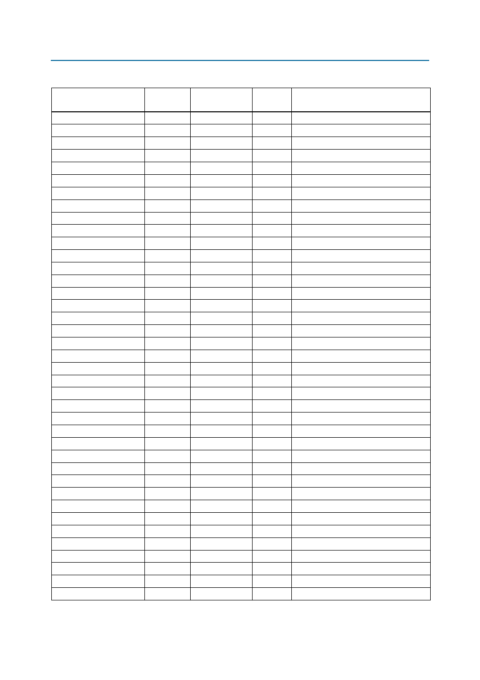
Table 2–5. MAX V CPLD System Controller Device Pin-Out (Part 3 of 6)
Schematic Signal Name
MAX V CPLD
Pin Number
Stratix V GS
Pin Number
I/O
Standard
Description