Cypress enCoRe CY7C63310 User Manual
Page 6
CY7C63310, CY7C638xx
Document 38-08035 Rev. *K
Page 6 of 83
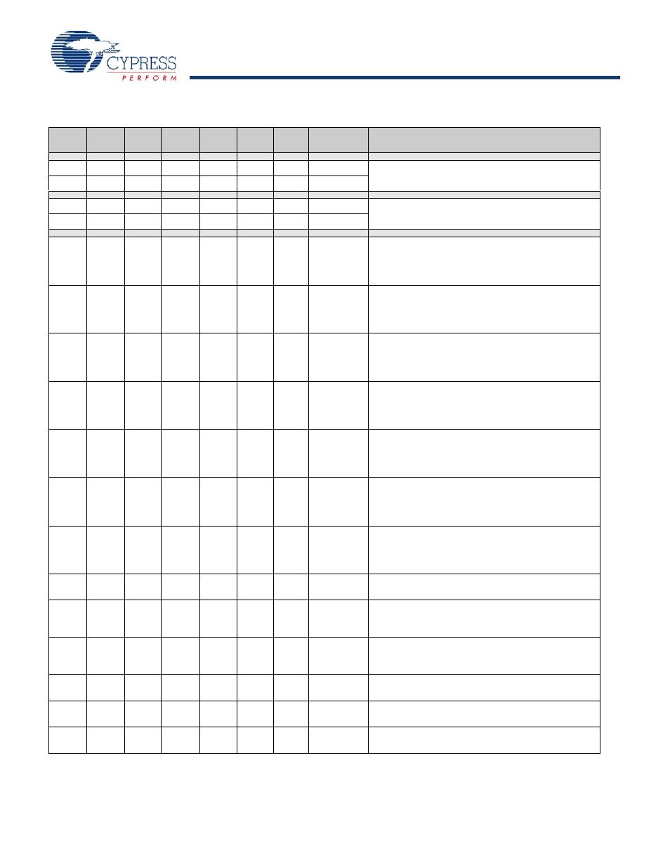
Table 5-2. Pin Description
32
QFN
24
QSOP
24
SOIC
18
SIOC
18
PDIP
16
SOIC
16
PDIP
Name
Description
21
19
18
P3.0
GPIO Port 3
. Configured as a group (byte).
22
20
19
P3.1
9
11
11
P2.0
GPIO Port 2
. Configured as a group (byte).
8
10
10
P2.1
14
14
13
10
15
9
13
P1.0/D+
GPIO Port 1 bit 0/USB D+
[1]
If this pin is used as a
General Purpose output, it draws current. This pin
must be configured as an input to reduce current
draw.
15
15
14
11
16
10
14
P1.1/D–
GPIO Port 1 bit 1/USB D–
If this pin is used as a
General Purpose output, it draws current. This pin
must be configured as an input to reduce current
draw.
18
17
16
13
18
12
16
P1.2/VREG GPIO Port 1 bit 2. Configured individually.
3.3V if regulator is enabled. (The 3.3V regulator is not
available in the CY7C63310 and CY7C63801.) A 1-
μF
min, 2-
μF max capacitor is required on Vreg output.
20
18
17
14
1
13
1
P1.3/SSEL GPIO Port 1 bit 3. Configured individually.
Alternate function is SSEL signal of the SPI bus TTL
voltage thresholds. Although Vreg is not available
with the CY7C63310, 3.3V IO is still available.
23
21
20
15
2
14
2
P1.4/SCLK GPIO Port 1 bit 4. Configured individually.
Alternate function is SCLK signal of the SPI bus TTL
voltage thresholds. Although Vreg is not available
with the CY7C63310, 3.3V IO is still available.
24
22
21
16
3
15
3
P1.5/SMOSI GPIO Port 1 bit 5. Configured individually.
Alternate function is SMOSI signal of the SPI bus TTL
voltage thresholds. Although Vreg is not available
with the CY7C63310, 3.3V IO is still available.
25
23
22
17
4
16
4
P1.6/SMISO GPIO Port 1 bit 6. Configured individually.
Alternate function is SMISO signal of the SPI bus TTL
voltage thresholds. Although Vreg is not available
with the CY7C63310, 3.3V IO is still available.
26
24
23
18
5
P1.7
GPIO Port 1 bit 7
. Configured individually.
TTL voltage threshold.
7
9
9
8
13
7
11
P0.0
GPIO Port 0 bit 0
. Configured individually.
On CY7C638xx and CY7C63310, external clock
input when configured as Clock In.
6
8
8
7
12
6
10
P0.1
GPIO Port 0 bit 1
. Configured individually.
On CY7C638xx and CY7C63310, clock output when
configured as Clock Out.
5
7
7
6
11
5
9
P0.2/INT0 GPIO Port 0 bit 2. Configured individually.
Optional rising edge interrupt INT0.
4
6
6
5
10
4
8
P0.3/INT1 GPIO Port 0 bit 3. Configured individually.
Optional rising edge interrupt INT1.
3
5
5
4
9
3
7
P0.4/INT2 GPIO Port 0 bit 4. Configured individually.
Optional rising edge interrupt INT2.
Note
1. P1.0(D+) and P1.1(D–) pins must be in IO mode when used as GPIO and in I
sb
mode.