2 command and response processing, 3 i2c cards, Command and response processing – Maxim Integrated 73S12xxF User Manual
Page 8: C cards, Figure 5: read command operations, Figure 6: write and security command operations, Figure 7: i, C data structure
Using Synchronous Smart Cards with the 73S12xxF
UG_12xxF_018
8
Rev. 1.0
2.2.2 Command and Response Processing
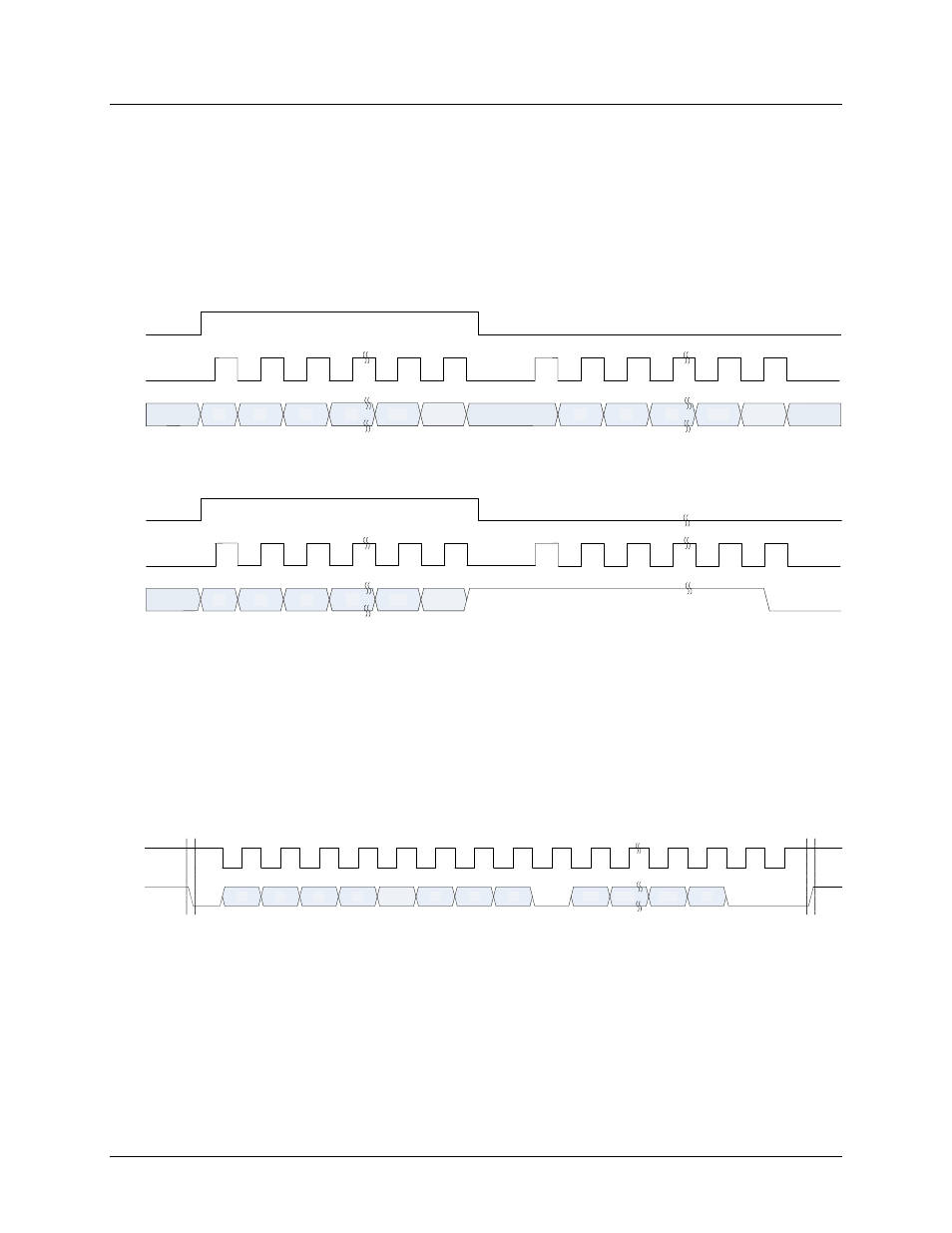
3-wire cards do not use start and stop bits. Instead they use the RST signal to frame the command
transactions. Like the 2-wire cards, the commands are formatted in the same manner as shown in
2. The command byte differs from the 2-wire cards in that it uses the two LSBs of the command byte as
address MSBs. As a result, the 3-wire cards have 10 bits of address so the size of the memory is 1K
bytes. The read operation is shown in
. As noted before, the write security operations take
some time to complete. Like the 2-wire cards, the processing time can be monitored as shown in
6 or a delay can be added to allow the processing to terminate before issuing the next command. The
write and security operations are shown in
C1
C3
C22
C23
1
2
3
24
C0
I/O
CLK
23
0
RST
C2
D0
D1
D2
Dn-1
Dn
Figure 5: Read Command Operations
C1
C3
C22
C23
1
2
3
24
C0
I/O
CLK
23
0
RST
C2
Figure 6: Write and Security Command Operations
2.3 I
2
C Cards
I
2
C cards do not support an ATR response. They operate similar to a 2-wire card where start and stop
bits are used. They do not use commands, but use a combination of the read/write bit and the start bit to
configure the type of operation to be performed. They do require the transmission of an I
2
C address and
a read/write bit for each transaction. In addition, an acknowledge (ACK) bit is required after transferring
every byte. For every byte transmitted by a sender an active low ACK bit must be sent by the receiver to
insure proper reception.
shows the data structure of a data packet.
D1
D2
D3
D4
D5
D6
D7
1
2
3
8
7
6
5
D0
I/O
CLK
4
9
ACK
STOP
START
D15
D14
ACK
Dn-1
Dn
Figure 7: I
2
C Data Structure
The first byte of a packet must contain the device address byte. The 6 MSB must hold the I
2
C device
address and contain a value of “1 0 1 0 0 0”. Bit 1 contains the MSB of the 17-bit address or a ‘0’ if data
is being read back on the following byte. Bit 0 contains the read/write bit.
shows the device
address. The device address will always begin with a start bit and be followed by either a memory
address or read data depending on the operation being performed. All write operations will require that
the memory address is specified in the second byte. Read operations can be configured to use the last
used address or use a command to write the address for the read and then read the actual data. This
application note only considers use of the read operations with the address specified.