Figure 22: i, C transaction end with stop bit, Figure 22 – Maxim Integrated 73S12xxF User Manual
Page 17
UG_12xxF_018
Using Synchronous Smart Cards with the 73S12xxF
Rev. 1.0
17
Figure 22: I
2
C Transaction End with Stop Bit
When reading data from the card, the device address has to be written to the card with or without the
memory address. If the R/W bit is set high, then the next byte after the ACK (designated as ACK
W
) will
be the first bit of the read data. If the R/W bit is low, then the memory address will follow the device
address. At the end of this frame and after the ACK bit, the CLK and the I/O should be stopped high to
prepare for the start bit that must precede any card read where the memory address is specified. The
device address must be sent again. This time with the R/W bit set high (for read). At this point, the data
can be read from the card.
Before reading data from the card, the ACK bit output (that follows the read data byte that will be
designated as ACK
R
) should be configured by setting the IOD for output and the I/O bit low. Waiting for
the WAITTO may be too late as the ISR has to be serviced and then the ACK
R
bit has to be set. To
ensure that the ACK
R
bit is output to the card immediately after the last data bit is read, the IOD and I/O
bits should be configured before the WAITTO interrupt is generated. Setting this during the ACK
W
bit
preceding the reading of the first bit of the read data stream may be too early. To insure all the ACKs are
properly configured, the first read ACK
R
bit should be configured somewhere in between these times.
This is easily accomplished by waiting at least 1 ETU after the WAITTO interrupt for the ACK
W
input that
precedes the first data read. By waiting for at least 1 ETU, the last ACK
W
bit is allowed to fully complete
before configuring the IOD and IO bits. When the WAITTO ISR is serviced, RLEN should be set for 9
which will automatically connect the I/O to the RX FIFO on the next falling edge of CLK. Waiting at least
1 ETU insures that this edge is output before configuring the IOD and IO bits. This method insures the
ACK bits are not during its bit time and the first ACK
R
is clean.
shows the proper format for an I
2
C read operation. It begins with a start bit followed by the
device address with the R/W bit set low to indicate that the memory address is to be written.
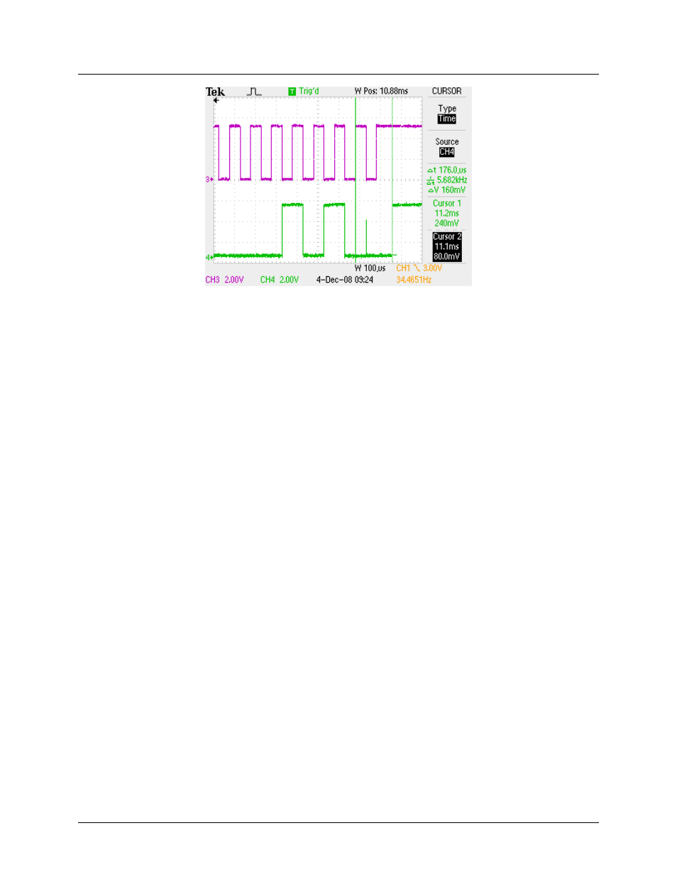
shows an example of a read operation. The left cursor shows the start bit followed by the device address
and a memory address of 0. After the memory address is written, another start bit is generated (note: no
stop was generated at the end of the memory address). The right cursor of
shows this start
bit. The device address is sent again, this time with the R/W bit set high to indicate that the data can now
be read from the card. After the ACK bit is verified, the smart card block is configured to receive data and
set RLEN to 9. Up to this point the operation of the ACK bit is the same as for the write operations.