3 reading data from the card, 3 i2c card operation, C card operation – Maxim Integrated 73S12xxF User Manual
Page 16: Figure 21: i
Using Synchronous Smart Cards with the 73S12xxF
UG_12xxF_018
16
Rev. 1.0
3.2.2.3 Reading Data from the Card
Reading data from a 3-wire card is a bit unusual. The CLK is low when the reading process begins.
When CLK starts, the first clock pulse is ignored. Refer to
to see this. This follows the same
logic as the smart card block and therefore doesn’t require any special processing except reading the
first byte must load RLEN with 9 and then 8 thereafter. The flowchart for reading data from a card is
shown in
.
3.2.3 I
2
C Card Operation
As mentioned above, the I
2
C cards operate similar to the 2-wire cards. They require the use of start and
stop bits to begin and end transactions. They differ in that they do not use specific commands or return
an ATR and require ACK and NAK bits as part of the protocol. The 73S12xxF smart card logic has
provisions for I
2
C operation and contains a control bit (I2CMODE in the STXCTL register) to configure the
smart card logic for I
2
C cards. By setting this control bit, the logic is configured to switch the I/O data from
the FIFOs to the I/O bit in the SCCtl (or SCECtl for the external interface) register when RLEN is reached
or is set to 0. When the interrupt is generated, the firmware must control the ACK bit manually through
I/O and IOD (I/O direction control) bits.
When sending data to the card every byte must be followed with a valid ACK from the card. The card will
set the ACK bit low after the last bit is sent. This occurs on the 9
th
falling edge of CLK. As a result, RLEN
should be set to 9 for all bytes read and written from/to a card.
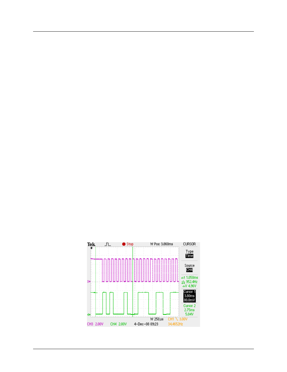
shows a transaction start with
device address and memory address. The left cursor shows the start bit. The right cursor shows the
ACK bit returned from the card. Notice that the bit preceding the ACK bit (R/W bit) is low so the next two
bytes must be the memory address. When a WAITTO interrupt is generated, the firmware must set the
IOD bit for input, write the next byte to the TX FIFO, set RLEN to 9 and set the IOD bit low so the ACK bit
can be read. The ACK bit should be sampled in the middle of the ACK bit so it should be sampled ½ ETU
after the interrupt. A proper ACK is low, so if the ACK bit is high, there is an error and the proper error
recovery algorithm should be executed. The CLK has not been stopped so the next falling edge of CLK
will automatically switch the I/O path back to the FIFO since the value of RLEN is no longer at the max
value or 0 (since it was reloaded). The setting of the IOD bit is overridden in the hardware so no
reconfiguration is required. At the beginning of the frame, the IOD bit is set for output to properly
configure the start bit. The IOD bit is overridden by hardware when the CLK is running and the value of
the RLEN counter is not at the limit or 0. At the end of a card write operation, the CLK should be stopped
high and the IOD bit should be set for output and I/O set low. A minimum 1 ETU delay should be allowed
for the CLK output to stop high and then the I/O should be taken high to create the stop bit.
shows a capture of the stop bit. The left cursor shows the last ACK and the right cursor shows the stop
bit. The I
2
C write data flow chart is shown in
Figure 21: I
2
C Transaction Start with Start Bit, Device Address and Memory Address