4 high sink, 5 open drain, 6 pull up enable – Cypress enCoRe CY7C602xx User Manual
Page 38: 7 output enable, 8 spi use, 9 p0.0/clkin configuration, Table 16-6
CY7C601xx, CY7C602xx
Document 38-16016 Rev. *E
Page 38 of 68
16.2.4 High Sink
When set, the output sinks up to 50 mA.
When clear, the output sinks up to 8 mA.
On the CY7C601xx, only the P3.7, P2.7, P0.1, and P0.0 have
50 mA sink drive capability. Other pins have 8 mA sink drive
capability.
On the CY7C602xx, only the P1.7–P1.3 have 50 mA sink drive
capability. Other pins have 8 mA sink drive capability.
16.2.5 Open Drain
When set, the output on the pin is determined by the Port Data
Register. If the corresponding bit in the Port Data Register is
set, the pin is in high impedance state; if it is clear, the pin is
driven LOW.
When clear, the output is driven LOW or HIGH.
16.2.6 Pull Up Enable
When set the pin has a 7K pull up to V
DD
.
When clear, the pull up is disabled.
16.2.7 Output Enable
When set, the output driver of the pin is enabled.
When clear, the output driver of the pin is disabled.
For pins with shared functions there are some special cases.
P0.0(CLKIN) and P0.1(CLKOUT) are not output enabled when
the crystal oscillator is enabled. Output enables for these pins
are overridden by XOSC Enable.
16.2.8 SPI Use
The P1.3(SSEL), P1.4(SCLK), P1.5(SMOSI), and
P1.6(SMISO) pins are used for their dedicated functions or for
GPIO. To enable the pin for GPIO, clear the corresponding SPI
Use bit. The SPI function controls the output enable for its
dedicated function pins when their GPIO enable bit is clear.
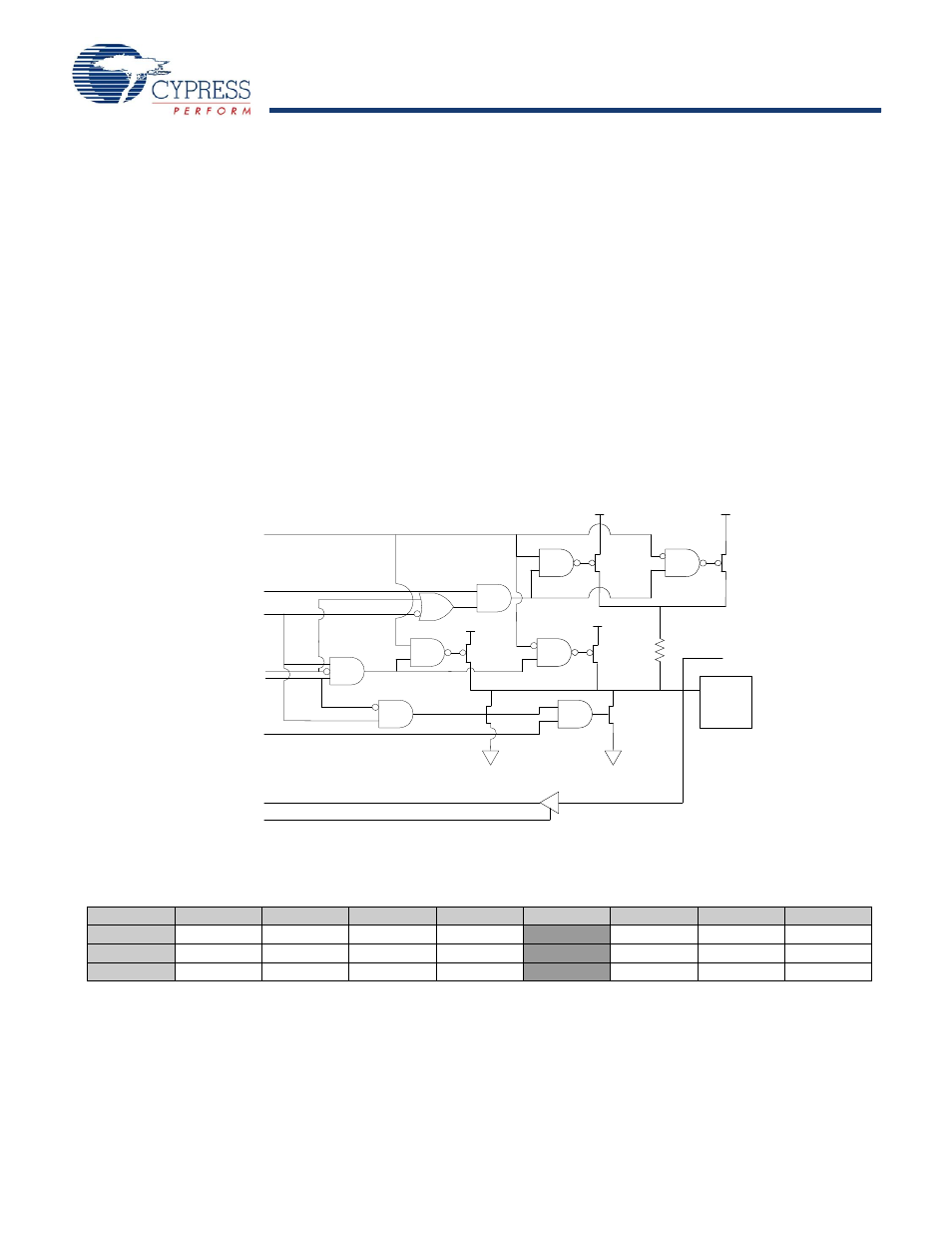
Figure 16-1. GPIO Block Diagram
16.2.9 P0.0/CLKIN Configuration
V
CC
VREG
V
CC
VREG
GPIO
PIN
R
UP
Data Out
V
CC
GND
VREG
GND
3.3V Drive
Pull-Up Enable
Output Enable
Open Drain
Port Data
High Sink
Data In
TTL Threshold
Table 16-6. P0.0/CLKIN Configuration (P00CR) [0x05] [R/W]
Bit #
7
6
5
4
3
2
1
0
Field
Reserved
Int Enable
Int Act Low
TTL Thresh
High Sink
Open Drain
Pull up Enable
Output Enable
Read/Write
–
R/W
R/W
R/W
R/W
R/W
R/W
R/W
Default
0
0
0
0
0
0
0
0
This pin is shared between the P0.0 GPIO use and the CLKIN pin for the external crystal oscillator. When the external oscillator
is enabled the settings of this register are ignored.
The alternate function of the pin as the CLKIN is only available in the CY7C601xx. When the external oscillator is enabled (the
XOSC Enable bit of the CLKIOCR Register is set—
), the GPIO function of the pin is disabled.
The 50 mA sink drive capability is only available in the CY7C601xx. In the CY7C602xx, only 8 mA sink drive capability is available
on this pin regardless of the setting of the High Sink bit.