15 p1.1 configuration, 16 p1.2 configuration, 17 p1.3 configuration (ssel) – Cypress enCoRe CY7C602xx User Manual
Page 41: Table 16-14

CY7C601xx, CY7C602xx
Document 38-16016 Rev. *E
Page 41 of 68
16.2.15 P1.1 Configuration
16.2.16 P1.2 Configuration
16.2.17 P1.3 Configuration (SSEL)
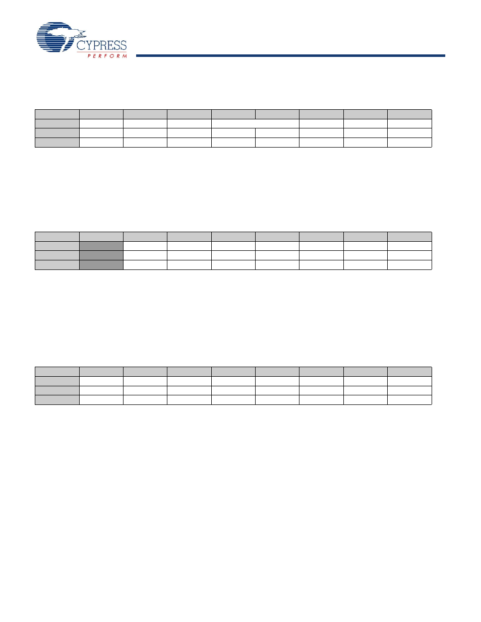
Table 16-12. P1.1 Configuration (P11CR) [0x0E] [R/W]
Bit #
7
6
5
4
3
2
1
0
Field
Reserved
Int Enable
Int Act Low
Reserved
Open Drain
Reserved
Output Enable
Read/Write
–
R/W
R/W
–
–
R/W
–
R/W
Default
0
0
0
0
0
0
0
0
This register controls the operation of the P1.1 pin.
The pull up resistor on this pin is enabled by the P10CR Register.
Note There is no 2 mA sourcing capability on this pin. The pin can only sink 5 mA at V
OL3
If this pin is used as a general purpose output, it draws current. It is, therefore, configured as an input to reduce current draw.
Table 16-13. P1.2 Configuration (P12CR) [0x0F] [R/W]
Bit #
7
6
5
4
3
2
1
0
Field
CLK Output
Int Enable
Int Act Low
TTL Threshold
Reserved
Open Drain
Pull up Enable
Output Enable
Read/Write
R/W
R/W
R/W
R/W
–
R/W
R/W
R/W
Default
0
0
0
0
0
0
0
0
This register controls the operation of the P1.2.
Bit 7: CLK Output
0 = The internally selected clock is not sent out onto P1.2 pin.
1 = This CLK Output is used to observe connected external crystal oscillator clock connected in CY7C601xx. When CLK Output
is set, the internally selected clock is sent out onto P1.2 pin.
Note:
on page 25 is used to select the external or internal clock in enCoRe II devices
Table 16-14. P1.3 Configuration (P13CR) [0x10] [R/W]
Bit #
7
6
5
4
3
2
1
0
Field
Reserved
Int Enable
Int Act Low
Reserved
High Sink
Open Drain
Pull Up Enable
Output Enable
Read/Write
–
R/W
R/W
–
R/W
R/W
R/W
R/W
Default
0
0
0
0
0
0
0
0
This register controls the operation of the P1.3 pin. This register exists in all enCoRe II LVparts.
The P1.3 GPIO’s threshold is always set to TTL.
When the SPI hardware is enabled or disabled, the pin is controlled by the Output Enable bit and the corresponding bit in the
P1 data register.
Regardless of whether the pin is used as an SPI or GPIO pin the Int Enable, Int act Low, High Sink, Open Drain, and Pull Up
Enable control the behavior of the pin.
