12 p0.5/tio0-p0.6/tio1 configuration, 13 p0.7 configuration, 14 p1.0 configuration – Cypress enCoRe CY7C602xx User Manual
Page 40: Table 16-9

CY7C601xx, CY7C602xx
Document 38-16016 Rev. *E
Page 40 of 68
16.2.12 P0.5/TIO0–P0.6/TIO1 Configuration
16.2.13 P0.7 Configuration
16.2.14 P1.0 Configuration
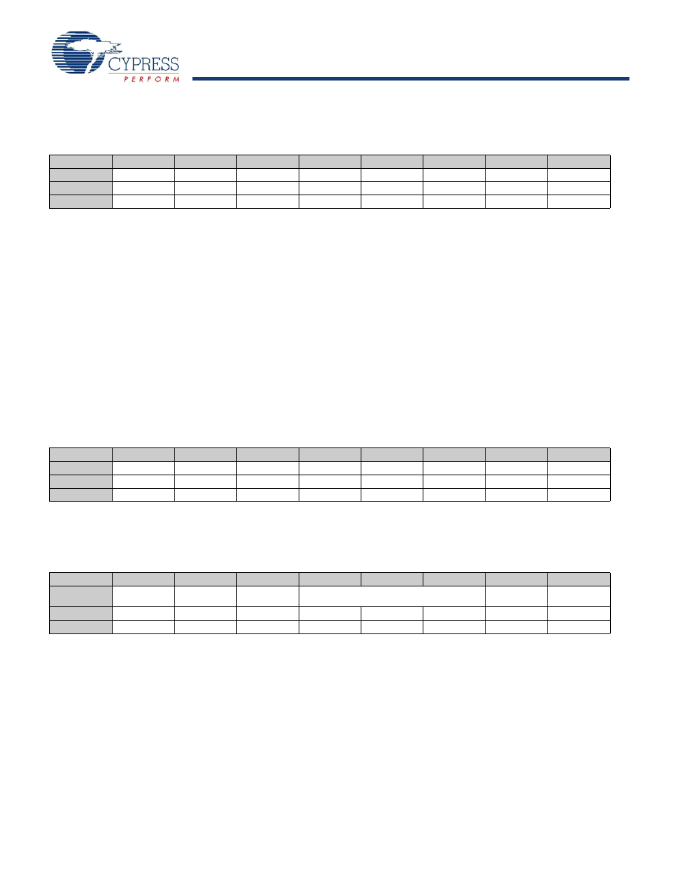
Table 16-9. P0.5/TIO0–P0.6/TIO1 Configuration (P05CR–P06CR) [0x0A–0x0B] [R/W]
Bit #
7
6
5
4
3
2
1
0
Field
TIO Output
Int Enable
Int Act Low
TTL Thresh
Reserved
Open Drain
Pull up Enable
Output Enable
Read/Write
R/W
R/W
R/W
R/W
–
R/W
R/W
R/W
Default
0
0
0
0
0
0
0
0
These registers control the operation of pins P0.5 through P0.6, respectively.
P0.5 and P0.6 are shared with TIO0 and TIO1 respectively. To use these pins as capture timer inputs, configure them as inputs
by clearing the corresponding Output Enable. To use TIO0 and TIO1 as timer outputs, set the TIOx Output and Output Enable
bits. If these pins are configured as outputs and the TIO Output bit is clear, firmware controls the TIO0 and TIO1 inputs by writing
the value to the P0.5 and P0.6 data bits in the P0 Data Register.
Regardless of whether either pin is used as a TIO or GPIO pin the Int Enable, Int Act Low, TTL Threshold, Open Drain, and Pull
up Enable control the behavior of the pin.
TIO0(P0.5) when enabled outputs a positive pulse from the 1024
μs interval timer. This is the same signal that is used internally
to generate the 1024
μs timer interrupt. This signal is not gated by the interrupt enable state. The pulse is active for one cycle
of the capture timer clock.
TIO1(P0.6) when enabled outputs a positive pulse from the programmable interval timer. This is the same signal that is used
internally to generate the programmable timer interval interrupt. This signal is not gated by the interrupt enable state.The pulse
is active for one cycle of the interval timer clock.
The P0.5/TIO0 and P0.6/TIO1 pins are individually configured with the P05CR (0x0A) and P06CR (0x0B), respectively.
Table 16-10. P0.7 Configuration (P07CR) [0x0C] [R/W]
Bit #
7
6
5
4
3
2
1
0
Field
Reserved
Int Enable
Int Act Low
TTL Thresh
Reserved
Open Drain
Pull up Enable
Output Enable
Read/Write
–
R/W
R/W
R/W
–
R/W
R/W
R/W
Default
0
0
0
0
0
0
0
0
This register controls the operation of pin P0.7.
Table 16-11. P1.0 Configuration (P10CR) [0x0D] [R/W]
Bit #
7
6
5
4
3
2
1
0
Field
Reserved
Int Enable
Int Act Low
Reserved
P1.0 and P1.1
Pull Up Enable
Output Enable
Read/Write
R/W
R/W
R/W
–
–
–
–
R/W
Default
0
0
0
0
0
0
0
0
This register controls the operation of the P1.0 pin.
Bit1: P1.0 and P1.1 Pull Up Enable
0 = Disable the P1.0 and P1.1 pull up resistors.
1 = Enable the internal pull up resistors for both the P1.0 and P1.1. Each of the P1.0 and P1.1 pins is pulled up with R
UP1
(see
Note There is no 2 mA sourcing capability on this pin. The pin can only sink 5 mA at V
OL3
The P1.0 is an open drain only output. It actively drives a signal low, but cannot actively drive a signal high.
If this pin is used as a general purpose output, it draws current. It is therefore configured as an input to reduce current draw.
