Low voltage detect control – Cypress enCoRe CY7C602xx User Manual
Page 34
CY7C601xx, CY7C602xx
Document 38-16016 Rev. *E
Page 34 of 68
15. Low Voltage Detect Control
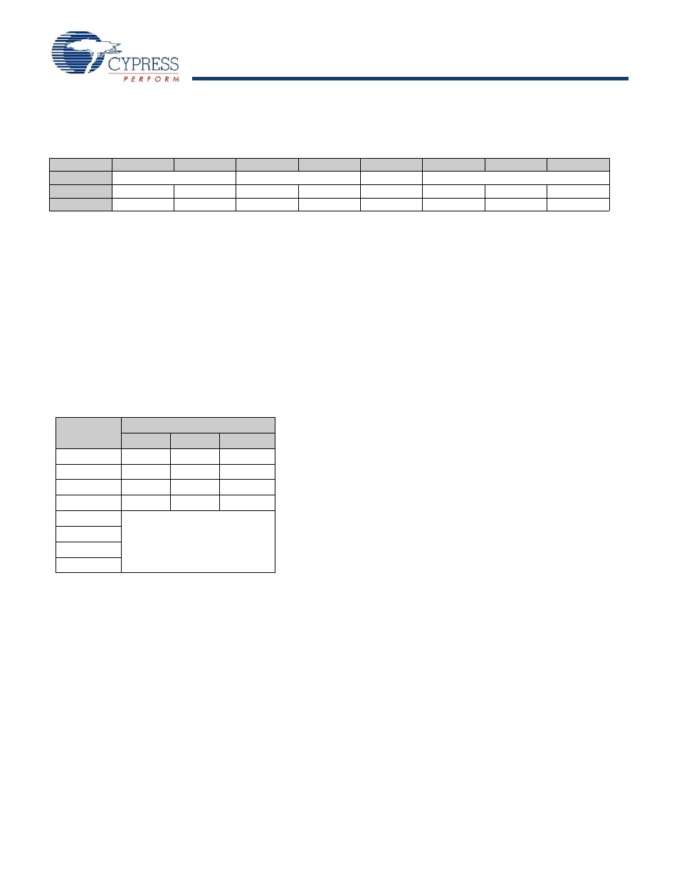
Table 15-1. Low Voltage Control Register (LVDCR) [0x1E3] [R/W]
Bit #
7
6
5
4
3
2
1
0
Field
Reserved
PORLEV[1:0]
Reserved
VM[2:0]
Read/Write
–
–
R/W
R/W
–
R/W
R/W
R/W
Default
0
0
0
0
0
0
0
0
This register controls the configuration of the Power on Reset and Low Voltage Detection circuit. This register is accessed only
in the second bank of IO space. This requires setting the XIO bit in the CPU flags register.
Bit [7:6]: Reserved
Bit [5:4]: PORLEV[1:0]
This field controls the level below which the precision power on-reset (PPOR) detector generates a reset.
0 0 = 2.7V Range (trip near 2.6V)
0 1 = 3V Range (trip near 2.9V)
1 0 = Reserved
1 1 = PPOR does not generate a reset, but values read from the Voltage Monitor Comparators Register (
) give the
internal PPOR comparator state with trip point set to the 3V range setting.
Bit 3: Reserved
Bit [2:0]: VM[2:0]
This field controls the level below which the low-voltage-detect trips—possibly generating an interrupt and the level at which
Flash is enabled for operation.
Note This register exists in the second bank of IO space. This requires setting the XIO bit in the CPU flags register.
VM[2:0]
LVD Trip Point (V)
Min
Max
Typical
000
2.69
2.72
2.7
001
2.90
2.94
2.92
010
3.00
3.04
3.02
011
3.10
3.15
3.13
100
Reserved
101
Reserved
110
Reserved
111
Reserved