Digilent FX12 User Manual
Page 8
Digilent
FX12 Reference Manual
www.digilentinc.com
Copyright Digilent, Inc.
Page 8/18
Doc: 502-046
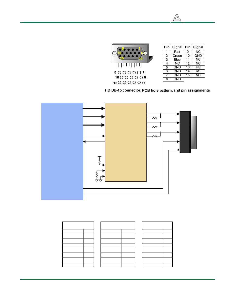
RED(7:0)
SYNC
CLK
RST
IC16
V6
See table
Analog Devices
ADV7125 Video
DAC
Virtex-4
FPGA
V5
See table
See table
GREEN(7:0)
BLUE(7:0)
BLANK
PSAVE
R
G
R_N
G_N
B
B_N
RED
GRN
BLU
HS
VS
V16
V15
HD-DB15
FX12 VGA Circuit Diagram
FPGA, and the inputs to those ports determine the corresponding color signal voltage delivered to the
VGA connector. The sync signals must be produced by a controller residing in the FPGA.
VGA signal timings are specified,
published, copyrighted and sold by the
VESA organization (www.vesa.org). The
following VGA system timing information
is provided as an example of how a
VGA monitor might be driven in 640 by
480 mode. For more precise
information, or for information on higher
VGA frequencies, refer to
documentation available at the VESA
website.
RED GREEN BLUE
RED7
V8 GREEN7 W10 BLUE75 W6
RED6
U9 GREEN6
Y11 BLUE6
W5
RED5
V9 GREEN5
W11 BLUE5
W7
RED4
V10 GREEN4
Y12 BLUE4
Y7
RED3
V11 GREEN3
W12 BLUE3
W8
RED2
V12 GREEN2
W13 BLUE2
W9
RED1
U1
GREEN1
T7
BLUE1
Y9
RED0
V13 GREEN0
U8
BLUE0
Y10