Digilent FX12 User Manual
Page 11
Digilent
FX12 Reference Manual
www.digilentinc.com
Copyright Digilent, Inc.
Page 11/18
Doc: 502-046
A VGA controller circuit decodes the output of a horizontal-sync counter driven by the pixel clock to
generate HS signal timings. This counter can be used to locate any pixel location on a given row.
Likewise, the output of a vertical-sync counter that increments with each HS pulse can be used to
generate VS signal timings, and this counter can be used to locate any given row. These two
continually running counters can be used to form an address into video RAM. No time relationship
between the onset of the HS pulse and the onset of the VS pulse is specified, so the designer can
arrange the counters to easily form video RAM addresses, or to minimize decoding logic for sync
pulse generation.
Signal Timings
LCD
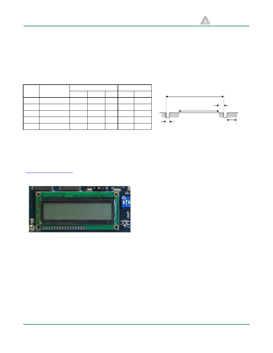
The FX12 contains a 16x2 character LCD manufactured by PowerTip (PN 1602D – see
www.powertip.com.tw
). The display uses an LCD controller IC compatible with the Samsung KS066U
and Sitronix ST7066U devices. All pins are routed directly to the Virtex FPGA as shown below.
The LCD controller contains a character-
generator ROM (CGROM) with 208 preset 5x8
character patterns, a character-generator RAM
(CGRAM) that can hold eight user-defined 5x8
characters, and a display data RAM (DDRAM)
that can hold 80 character codes. Character
codes written into the DDRAM serve as indexes
into the CGROM (or CGRAM). Writing a character
code into a particular DDRAM location will cause
the associated character to appear at the corresponding display location. Display positions can be
shifted left or right by setting a bit in the instruction register (IR). The write-only IR directs display
operations (such as clear display, shift left or right, set DDRAM address, etc). Available instructions
(and the associated IR codes) are shown in the right-most column of the “LCD Instructions and
Codes” table below. A busy flag shows whether the display has competed the last requested
operation; prior to initiating a new operation, the flag can be checked to see if the previous operation
has been completed.
The display has more DDRAM locations than can be displayed at any given time. DDRAM locations
00H to 27H map to the first display row, and locations 40H to 67H map to the second row. Normally,
DDRAM location 00H maps to the upper left display corner, and 40H to the lower left. Shifting the
display left or right can change this mapping. The display uses a temporary data register (DR) to hold
data during DDRAM /CGRAM reads or writes, and an internal address register to select the RAM
location. Address register contents, set via the IR, are automatically incremented after each read or
write operation. The LCD display uses ASCII character codes. Codes up through 7F are standard
T
S
T
disp
T
pw
T
fp
T
bp
T
S
T
disp
T
pw
T
fp
T
bp
Sync pulse time
Display time
VS pulse width
VS front porch
VS back porch
16.7ms
15.36ms
64 us
320 us
928 us
416,800
384,000
1,600
8,000
23,200
521
480
2
10
29
Symbol
Parameter
Time
Clocks Lines
Vertical Sync
32 us
25.6 us
3.84 us
640 ns
1.92 us
800
640
96
16
48
Clocks
Horizontal Sync
Time