Digilent FX12 User Manual
Page 5
Digilent
FX12 Reference Manual
www.digilentinc.com
Copyright Digilent, Inc.
Page 5/18
Doc: 502-046
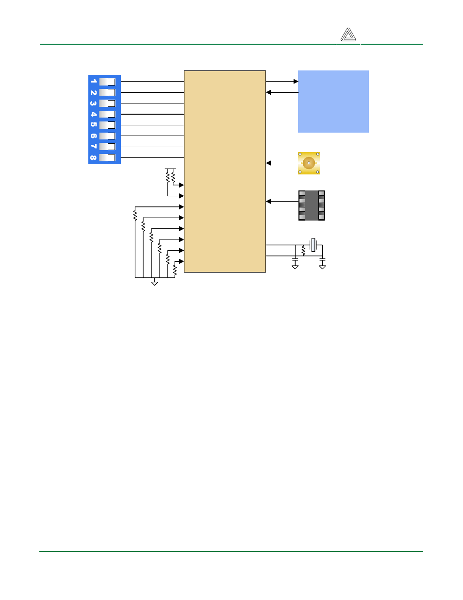
IC15
R18 (GCLK0)
ICS8402
Frequency
Synthesizer
Virtex-4
FPGA
Q1
XTAL_SEL
OE1
R18
M0
M1
M2
M3
M4
N0
N1
VCO_SEL
OE2
M5
M7
M6
M8
NP_LOAD
MR
25MHz
Crystal
XTAL1
XTAL2
Q0
TEST_CLK
SMA
Connector
Test
Clock
Socket
Frequency
Select
Switches
FX12 Frequency Synthesizer Diagram
DDR
The 64Mbyte DDR memory array consists of two 32Mbyte (16M x 16) ISSI IS43R16160A-6T devices
connected as a 16M x 32 array. Individual byte selects for both memories are brought to the FPGA so
byte, word, and long-word read/writes are possible. A differential clock is routed from the FPGA to the
memories, and a length-matched clock return is routed back to the FPGA to allow for timing
optimization. All data signals are delay and impedance matched (with 48-ohm trace impedance), and
all DDR signals are actively terminated through 47-ohm resistors to a 1.25V supply for optimal bus
performance.
UCF File
Signals routed to the DDR SDRAM should use the SSTL2_I standard as shown in the example .ucf
file entry below. All VREF pins on Bank 5 (used by the DDR signal connections) should have “prohibit”
constraints in the .ucf file to prohibit software from assigning these pins to other functions.
NET
“DDR_D0”
LOC
= “P20” |
IOSTANDARD
= SSTL2_I ;
CONFIG
PROHIBIT
= C17;