Digilent FX12 User Manual
Page 3
Digilent
FX12 Reference Manual
www.digilentinc.com
Copyright Digilent, Inc.
Page 3/18
Doc: 502-046
FX12 Stack-Up
Layer Usage Copper
1 Signal 1
oz.
2 GND .5
oz.
3 Signal .5
oz.
4 Vdd .5
oz.
5 Vdd .5
oz.
6 Signal .5
oz.
7 GND .5
oz.
8 Signal 1
oz.
After the Platform Flash ROM has been loaded with a configuration file, the FPGA can load that file at
power-on if the mode select jumpers are set in the Platform Flash position.
An FPGA system-reset button labeled PROG has been provided to allow a user-initiated FPGA reset.
Pressing the PROG button will clear all configuration memory and cause the FPGA to await the next
programming cycle. An LED on the DONE signal will illuminate at the end of a successful
configuration.
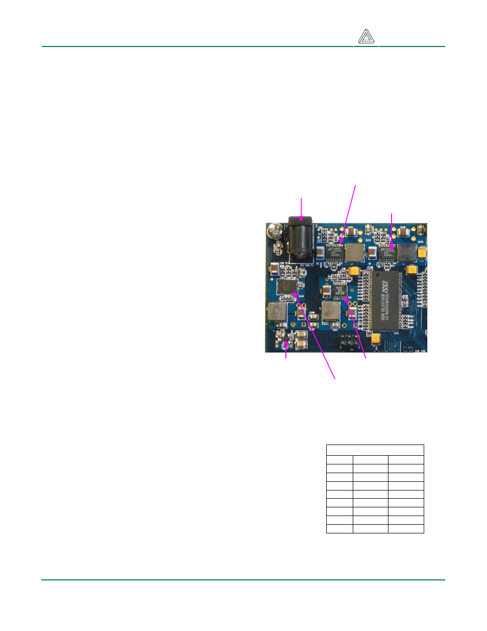
Power Supplies
Power is delivered to the FX12 board via a 2.1mm,
center-positive power connector that can be driven
from any suitable 4VDC-5.5VDC source (like a
wall-plug supply). Power is routed from the
connector to four switching regulators and single
LDO that produce all required supply voltages.
Input power is also routed directly to the character
LCD and high-speed expansion connector (pins
A49 and A50) for use by peripheral circuits.
Current Consumption
Total board current is dependant on FPGA
configuration, synthesizer clock frequency, and
external connections. In test configurations using
the PPC core to run DDR and Flash memory tests,
with roughly 10% of the FPGA routed and a
100MHz input clock, approximately 650mA of
supply current is drawn from the main power
supply. Required current will increase if larger
circuits are configured in the FPGA, if clock
frequency is increased, and if peripheral boards are
attached.
Power Distribution
The FX12 uses an eight-layer PCB, with the stack-up shown in the
table. The Vdd planes are split into several localized islands to
accommodate the various component’s supply voltage requirements.
Bulk ceramic bypass capacitors are placed strategically around the
board, and every component Vdd pin has one, two, or three local
bypass caps in the .001 to .047uF range. The power supply routing
and bypass capacitors result in a very clean low-noise power supply.
Supply Details
3.3V switching supply
for FPGA I/O and
peripherals (LTC3416)
2.5V switching supply
for DDR (LTC3416)
1.2V switching supply for
FPGA core (LTC3418)
1.25V switching supply for
DDR termination (LTC3413)
2.1mm center-
positive power jack
1.8V LDO for
Platform Flash
ROM (LTC1844)
FX12 Power Supplies