Digilent FX12 User Manual
Page 12
Digilent
FX12 Reference Manual
www.digilentinc.com
Copyright Digilent, Inc.
Page 12/18
Doc: 502-046
ASCII (which includes all “normal” alphanumeric characters). Codes above 7F produce various
international characters – please see the manufacturers data sheet for more information on
international codes.
The display is connected to the FX12 board by a 16-pin connector (pins 15 and 16 are for an optional
backlight, and they are not used). The 14-pin interface includes eight data signals, three control
signals, and three voltage supply signals. The eight data bus signals are passed through the CPLD
to/from the system bus for read/write cycles directed to the LCD memory space (address 10X). The
three LCD control signals are driven from the CPLD: the RS (Register Strobe) signal clocks data into
registers, the R/W signal determines bus direction, and the E signal enables the bus for read or write
operations. In the standard CPLD configuration, the R/S and R/W signals are connected to ADDR0
and WE respectively. The E signal can be driven directly from the LCDEN signal available on the
system connector, or if LCDEN is left at logic ‘0’, then E is driven whenever address “10X” is present
on the bus, CS is asserted, and AS or DS are low. LCD bus signals and timings are illustrated below.
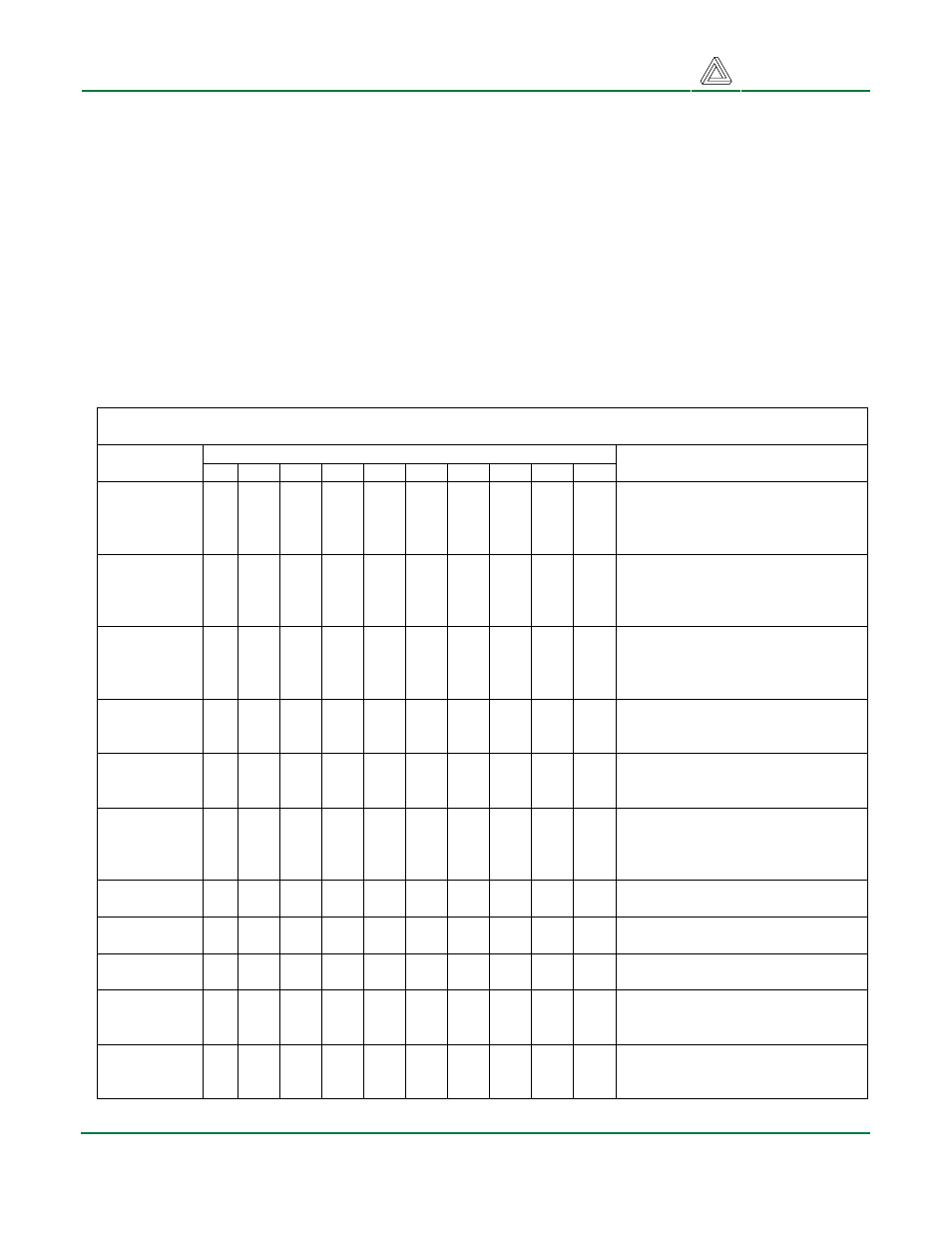
LCD Instructions and Codes
Instruction Bit Assignments
Instruction
RS R/W DB7 DB6 DB5 DB4 DB3 DB2 DB1 DB0
Description
Clear
Display
0 0 0 0 0 0 0 0 0 1
Clear display by writing a 20H to
all DDRAM locations, set DDRAM
address register to 00H, and
return cursor to home.
Return
Home
0 0 0 0 0 0 0 0 1 X
Return cursor to home (upper left
corner), and set DDRAM address
to 0H. DDRAM contents not
changed.
Entry Mode
Set
0 0 0 0 0 0 0 1 I/D
SH
I/D = ‘1’ for right-moving cursor
and address increment, SH = ‘1’
for display shift (direction set by
I/D bit).
Display
ON/OFF
Control
0 0 0 0 0 0 1 D C B
Set display (D), cursor (C), and
blinking cursor (B) on or off.
Cursor or
Display Shift
0 0 0 0 0 1 S/C
R/L
X X
SC = ‘0’ to shift cursor right or left,
‘1’ to shift entire display right or
left (R/L = ‘1’ for right).
Function
Set
0 0 0 0 1 DL
N F X X
Set interface data length (DL = ‘1’
for 8 bit), number of display lines
(N = ‘1’ for 2 lines), display font (F
= ‘0’ for 5x 8 dots).
Set CGRAM
Address
0 0 0 1
AC5 AC4 AC3 AC2 AC1 AC0 Set
CGRAM
address
counter.
Set DDRAM
Address
0
0
1
AC6 AC5 AC4 AC3 AC2 AC1 AC0 Set DDRAM address counter.
Read Busy
Flag/ Address
0 1 BF
AC6
AC5 AC4 AC3 AC2 AC1 AC0
Read busy flag and address
counter.
Write Data
to RAM
1 0 D7 D6 D5 D4 D3 D2 D1 D0
Write data into DDRAM or
CGRAM, depending on which
address was last set.
Read Data
from RAM
1 1 D7 D6 D5 D4 D3 D2 D1 D0
Read data from DDRAM or
CGRAM, depending on which
address was last set.