Digilent FX12 User Manual
Page 14
Digilent
FX12 Reference Manual
www.digilentinc.com
Copyright Digilent, Inc.
Page 14/18
Doc: 502-046
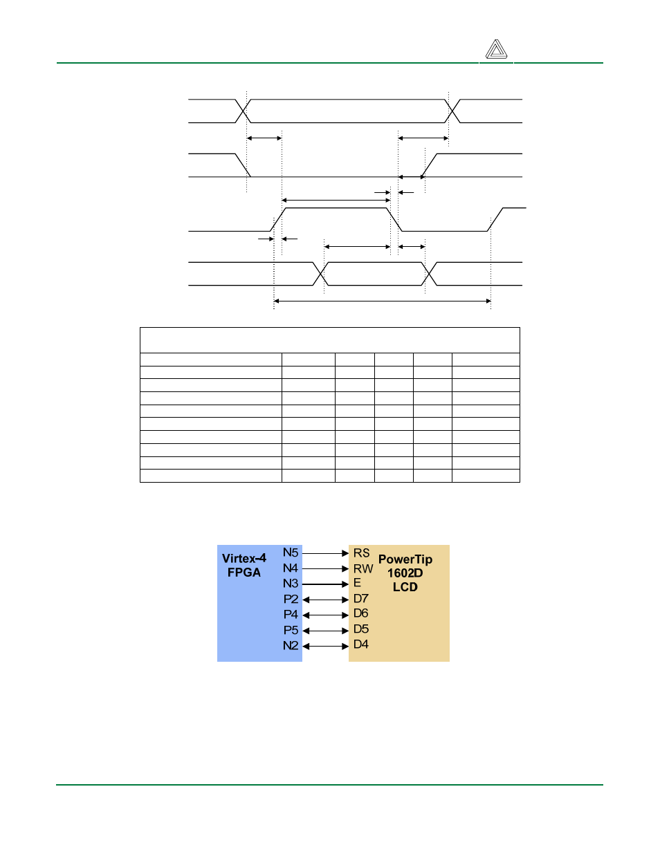
LCD Write Cycle
tsu
th
th
tw
tr
tf
tsu1
th1
tc
R/ W
RS
E
DB0- DB7
The LCD connections to the Virtex-4 are shown below. Note the LCD uses a 4-bit data interface, and
the same FPGA pins that connect to the data bus are shared with the pushbutton inputs.
FX12 LCD Circuit Diagram
Serial Port
The FX12 provides an RS-232 based serial port for user data transfers and embedded processor debug
operations. RS-232 level translation is provided by an Intersil ICL3232 transceiver.
LCD Bus Timings
Parameter Symbol
Min
Max
Unit
Test
Pin
Enable cycle time
tc
500
ns
E
Enable High pulse width
tw
220
ns
E
Enable rise/fall time
tr, tf
25
ns
E
RS, R/W setup time
tsu
40
ns
RS, R/W
RS, R/W hold time
th
10
ns
RS, R/W
Read data output delay
td
60
120
ns
DB0-DB7
Read data hold time
tdh
20
ns
DB0-DB7
Write data setup time
tsu1
40
ns
DB0-DB7
Write data hold time
th1
10
ns
DB0-DB7
- 410-282P-KIT (4 pages)
- 410-279P-KIT (26 pages)
- 410-258P-KIT (16 pages)
- 410-138P-KIT (28 pages)
- 410-178P-KIT (22 pages)
- 410-292P-KIT (29 pages)
- 410-274P-KIT (29 pages)
- 410-182P-KIT (22 pages)
- 410-134P-KIT (17 pages)
- 410-183P-KIT (19 pages)
- 410-155P-KIT (12 pages)
- 6015-410-001P-KIT (26 pages)
- 410-087P-KIT (164 pages)
- 410-146P-KIT (4 pages)
- 6003-410-000P-KIT (138 pages)
- XUPV2P (23 pages)
- 410-047-C2P-KIT (3 pages)
- WaveForms (85 pages)
- 410-297P-KIT (25 pages)
- 410-295P-KIT (37 pages)
- 410-296P-KIT (23 pages)
- 410-209P-KIT REV.D (16 pages)
- 410-209P-KIT REV.C (17 pages)
- 410-254P-KIT (17 pages)
- 410-280P-KIT (9 pages)
- 410-202P-KIT (20 pages)
- 410-273P-KIT (24 pages)
- 410-269P-KIT (11 pages)
- 410-216P-KIT (15 pages)
- 410-231P-KIT (4 pages)
- 410-211P-KIT (10 pages)
- 410-262P-KIT (8 pages)
- 410-229P (7 pages)
- 410-242P-KIT (4 pages)
- 6021-210-000P-KIT (27 pages)
- 410-185P-KIT (21 pages)
- 6032-410-000P-BOARD (4 pages)
- 410-174P (17 pages)
- 410-145P (6 pages)
- 210-264P-BOARD (3 pages)
- 6003-210-012P (27 pages)
- 410-236P-BOARD (2 pages)
- 410-163P (1 page)
- 410-097P-KIT (2 pages)
- 410-255P-KIT (1 page)