Digilent DIO5 User Manual
Page 8
DIO5 Reference Manual
Digilent, Inc.
www.digilentinc.com
Page
8
Copyright Digilent, Inc. All rights reserved. Other product and company names mentioned may be trademarks of their respective owners.
When configured with the code shown in the
appendix, the CPLD on the DIO5 board
implements a seven-segment controller
provided a suitable clock (256Hz to 1KHz) is
provided on the LCLK pin. The controller
accepts four 4-bit binary numbers in two
successive registers, and decodes and
displays them.
Discrete LEDs
Sixteen individual LEDs (5
green, 5 yellow, and 6 red)
are provided for circuit
outputs. The LED cathodes
are driven directly from the
CPLD, and the anodes are
tied to Vdd via 390-ohm
resistors (so the LED drive
signals are active low).
When the CPLD is
configured with the code
shown in the appendix, two 8-bit registers (at
writable locations 000 and 001 in the CPLD)
drive the LED cathode signals. Note the LED
signals are inverted in the VHDL code, so a
logic “1” turns on the LEDs.
Pushbutton Inputs
Outputs from the 16 momentary-contact push
buttons are normally low, and are driven high
only while the button is actively pressed. The
buttons exhibit a worst-case bounce time of
about 1ms. A 4.7K series resistor provides
some debounce filtering and ESD protection to
each button. When configured with the code
shown in the appendix, the CPLD on the DIO5
board makes all button signals available on the
bus in two successive readable address
locations (0 and 1).
Switch Inputs
The eight slide switches on the DIO5 can be
used to connect either Vdd or GND to eight pins
on the CPLD. The switches exhibit about 2ms of
bounce, and no active debouncing circuit is
employed. A 4.7K-ohm series resistor is used for
nominal input protection. When configured with
the code shown in the appendix, the CPLD
makes all switch signals available on the system
bus at address location 2.
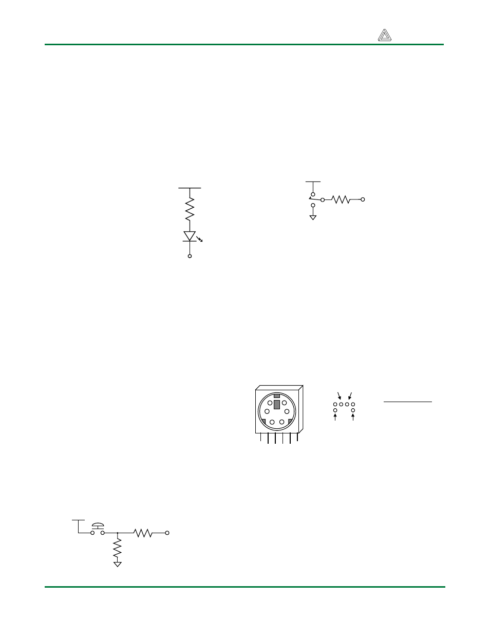
PS2 Port
The DIO5 board includes a 6-pin mini-DIN
connector that can accommodate a PS2 mouse
or PS2 keyboard connection. A 5VDC regulator
provides the required voltage to keyboards
and/or mice. Both the mouse and keyboard use
a two-wire serial bus (including clock and data)
to communicate with a host device. These
signals are routed through the CPLD to provide
voltage mapping, and to allow a controller to be
placed in the CPLD.
PS2 Connector
Pin 1
Pin 5
Pin 6
Bottom-up
hole pattern
Pin Definitions
Pin Function
1 Data
2 Reserved
3 GND
4 Vdd
5 Clock
6 Reserved
1
5
3
2
4
6
Pin 2
The keyboard and mouse both use identical
signal timings. Both use 11-bit words that include
a start, stop and odd parity bit, but the data
packets are organized differently, and the
keyboard interface allows bi-directional data
transfers (so the host device can illuminate state
LEDs on the keyboard). Bus timings are shown
below. The clock and data signals are only
driven when data transfers occur, and otherwise
they are held in the “idle” state at logic ‘1’. The
timings define signal requirements for mouse-to-
Vdd
LD# signal
39
0
GND
Vdd
SW#
signal
4.7K
Ω
Vdd
GND
4.7K
Ω
4.7K
Ω
BTN#
signal