Digilent DIO5 User Manual
Page 3
DIO5 Reference Manual
Digilent, Inc.
www.digilentinc.com
Page
3
Copyright Digilent, Inc. All rights reserved. Other product and company names mentioned may be trademarks of their respective owners.
latches. These ten signals are always available
regardless of the system bus state.
The CPLD also contains a seven-segment
display controller. Binary data, in the form of
four 4-bit fields spanning two bytes, can be
written to the seven-segment data registers
and it will be displayed as four hexadecimal
characters on the seven-segment display. The
display controller uses LCLK to control refresh
timing.
Bi-directional LCD data transfers occur over
the system bus. The default CPLD circuit
synthesizes LCD control signals for bus cycles
directed to the LCD memory space, but it is
also possible to drive the LCD control signals
directly. The “LCD” section below provides
information on driving the LCD.
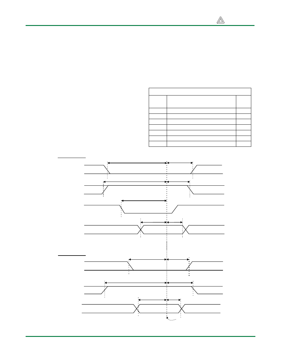
System bus timings are shown below. Data is
written on the rising edge of write-enable (WE).
DIO5 bus drivers are enabled whenever output
enable (OE) is asserted (low). The diagrams
below show signal timings assumed by Digilent
to create peripheral devices. Different bus and
timing models can be used by modifying
circuits in the FPGA and attached peripheral
devices.
System Bus Timings
Symbol
Parameter
Time
(typ)
ten
Time to enable after CS asserted 10ns
th Hold
time
1ns
tdoe Disable time after OE deasserted 10ns
teoe Enable time after OE asserted
15ns
tw
Write strobe time
10ns
tsu
Data setup time
5ns
twd
Write disable time
0ns
tw
th
OE
CS
WE
DB0-DB7
th
teoe
tsu
tdoe
twd
th
OE
WE
DB0-DB7
teoe
tsu
tdoe
ten
Read data latch time
th
Write Cycle
Read Cycle
System Bus Timing