Digilent DIO5 User Manual
Page 2
DIO5 Reference Manual
Digilent, Inc.
www.digilentinc.com
Page
2
Copyright Digilent, Inc. All rights reserved. Other product and company names mentioned may be trademarks of their respective owners.
supply is used to drive the CPLD and all other
I/O devices on the board. During normal
operation, the DIO5 consumes 10-20mA from
the 5V supply, and 50-100mA from the 3.3V
supply depending on how many LEDs are
illuminated. The DIO5 uses a four-layer board,
with two layers dedicated to 3.3V and GND,
and several bulk and high-frequency
decoupling capacitors to keep the supplies
stable under all loads.
CPLD Configuration
The JTAG scan chain is routed through the
DIO5 board on pins 1-4 of connector P1,
allowing the CPLD to be configured from any
Digilent system board. Jumper-shunts must be
loaded on pins 1 & 2 of jumper blocks JP2 and
JP3 on the DIO5 to include the CPLD in the
scan chain, or across pins 2 & 3 to remove the
CPLD from the scan chain.
Jumper position JP1 allows the JTAG signals
on the CPLD to be reclaimed if they are
inadvertently programmed as user I/O’s. Since
the JTAG pins on the CPLD are used only for
programming, this jumper block should not
normally be loaded. The CPLD pinout is
available in appendix 1.
System Board Interface
Signals from all I/O devices on the DIO5 are
routed through the CPLD, with the exception of
the VGA port (video data is too high bandwidth
to pass through the CPLD). All I/O devices on
the DIO5 can therefore be read or written via a
register-based controller in the CPLD. Some
device signals, including the eight slide
switches, the PS/2 data and clock, and an LCD
enable are also routed around the CPLD and
directly to the connectors. These signals can
be accessed either through the CPLD or
directly from the system board.
The CPLD offers several options for moving
data between the DIO5 and a system board: a
memory-mapped bus interface can be defined
where all devices are accessed via registers; a
“direct connect” interface can be defined where
I/O signals pass directly through the CPLD
without the need for a bus (in this case, not all
devices on the DIO5 can be accessed); or
various controllers and compression/encoding
schemes can be used to transfer device data
over subsets of pins.
The default DIO5 CPLD circuit defines a
“system bus” to transfer data to and from a
system board. The bus uses 8 bi-directional
data lines, six address lines, three control
signals, and a clock signal (LCLK). The three
control signals, write enable (WE), output
enable (OE), and chip select (CS), are used to
coordinate bus traffic, and the LCLK signal
provides a clock for latches and controllers on
the DIO5. Four 8-bit write-only registers are
used to receive LED and seven-segment
display data in the CPLD, and three readable
locations contain pushbutton and switch data.
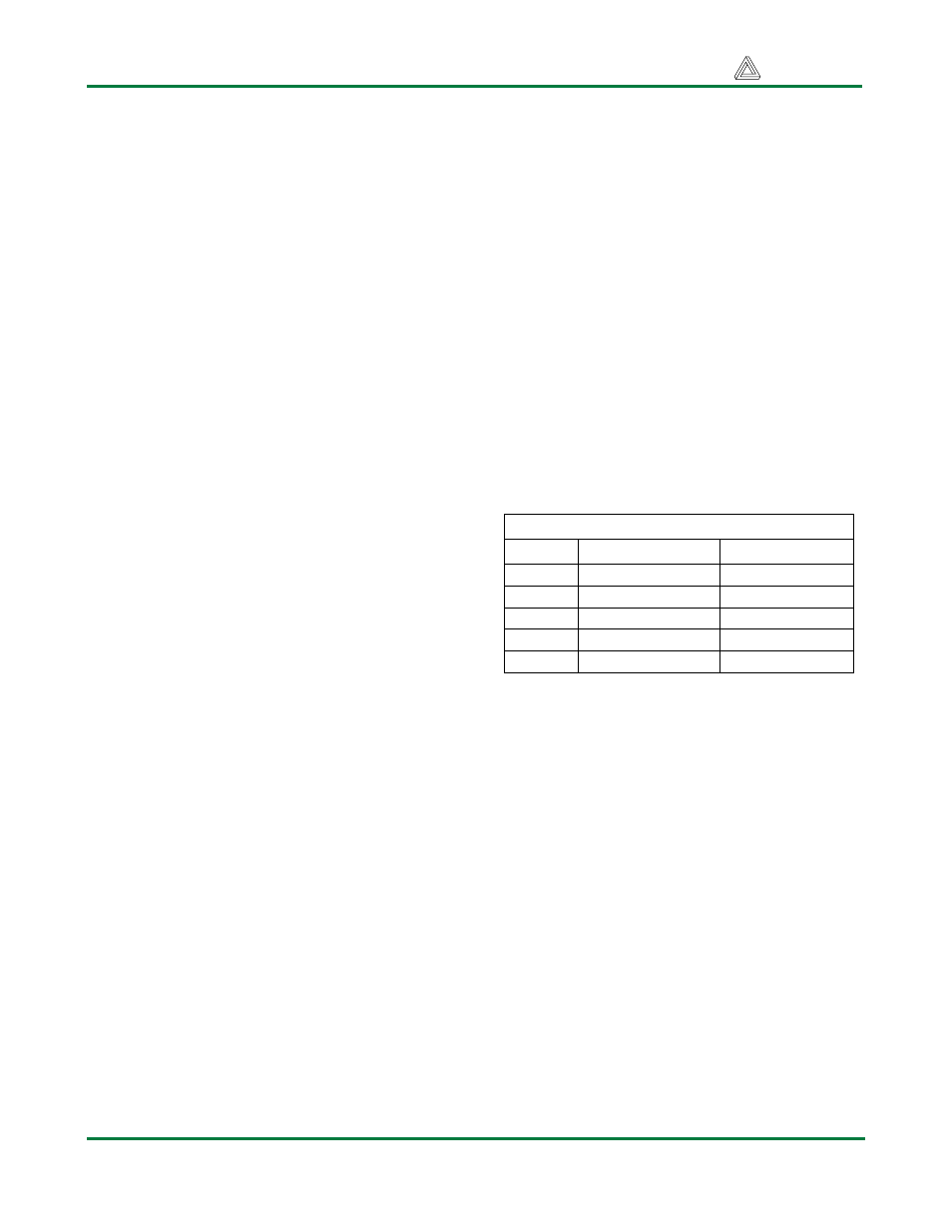
DIO5 Default Circuit Memory Map
Address
Read Write
000
BtnLo (buttons 0-7) LedLo (LEDs 0-7)
001
BtnHi (buttons 8-F) LedHi (LEDs 8-F)
010
Swt (slide switches) SsegLo
011 unused
SsegHi
10X
LCD bus
LCD bus
Two read locations, BtnHi and BtnLo, arise
from latches in the CPLD. Pushbutton signals
are stored in these two 8-bit latches at each
rising edge of LCLK. The third read location,
Swt, simply passes switch signals to the
system bus from the switch input pins.
The four writable registers in the CPLD all
provide data to the LED devices (i.e., the
seven-segment displays and discrete LEDs).
The registers use rising-edge-triggered flip-
flops clocked by the trailing edge of the write
enable signal (WE is active low). Data written
to these registers appears immediately on the
LED’s.
Ten additional pushbutton signals bypass the
system bus, and are routed from the CPLD
directly to pins on the expansion connectors.
Four of these signals contain BCD codes for
buttons 0-9, and six signals are simply the
state of buttons A-F at the output of the