Digilent DIO5 User Manual
Page 5
DIO5 Reference Manual
Digilent, Inc.
www.digilentinc.com
Page
5
Copyright Digilent, Inc. All rights reserved. Other product and company names mentioned may be trademarks of their respective owners.
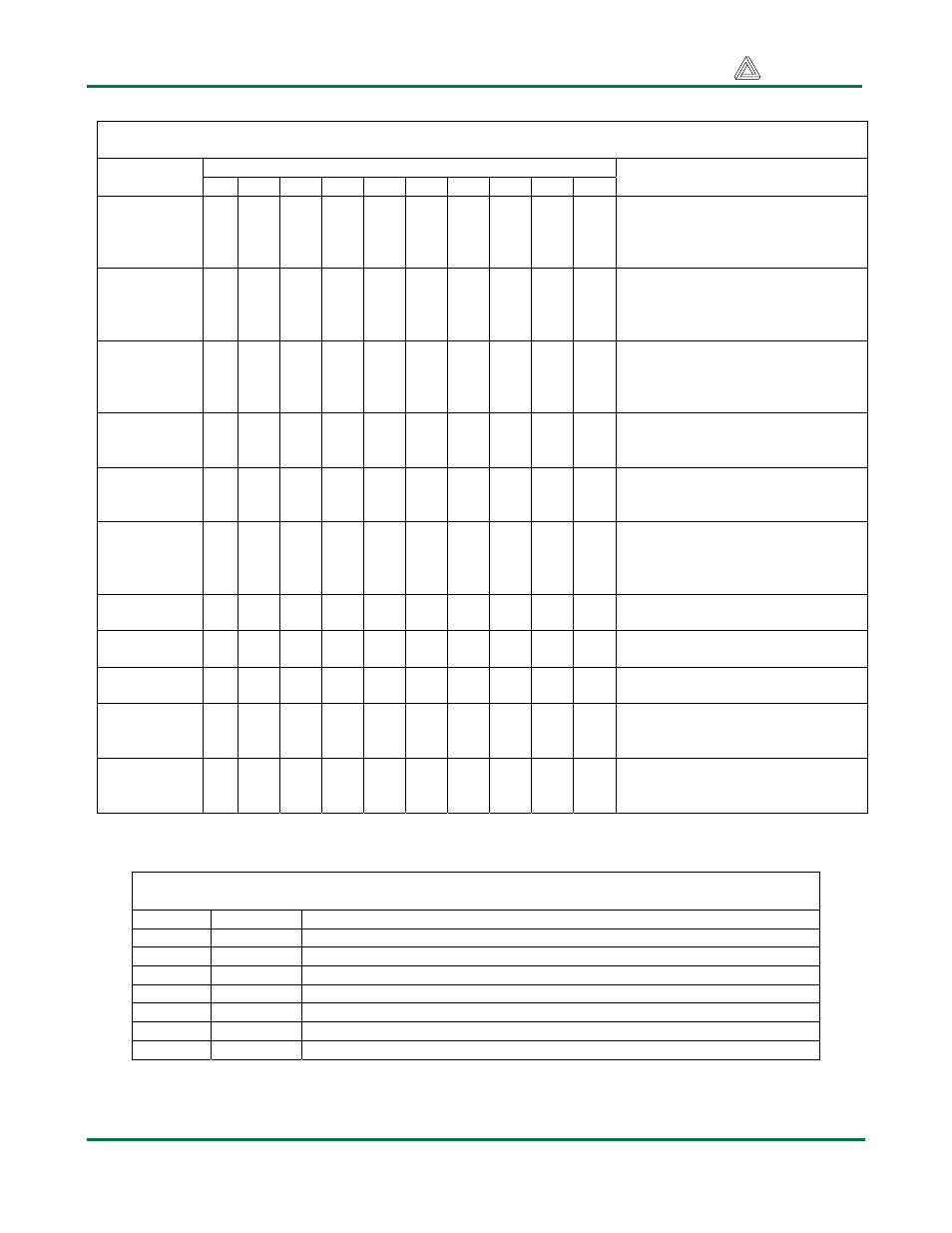
Table 3. LCD Instructions and Codes
Instruction bit assignments
Instruction
RS R/W DB7 DB6 DB5 DB4 DB3 DB2 DB1 DB0
Description
Clear
Display
0 0 0 0 0 0 0 0 0 1
Clear display by writing a 20H to
all DDRAM locations; set DDRAM
address register to 00H; and
return cursor to home.
Return
Home
0 0 0 0 0 0 0 0 1 X
Return cursor to home (upper left
corner), and set DDRAM address
to 0H. DDRAM contents not
changed.
Entry mode
set
0 0 0 0 0 0 0 1 I/D
SH
I/D = ‘1’ for right-moving cursor
and address increment; SH = ‘1’
for display shift (direction set by
I/D bit).
Display
ON/OFF
control
0 0 0 0 0 0 1 D C B
Set display (D), cursor (C), and
blinking cursor (B) on or off.
Cursor or
Display shift
0 0 0 0 0 1 S/C
R/L
X X
SC = ‘0’ to shift cursor right or left,
‘1’ to shift entire display right or
left (R/L = ‘1’ for right).
Function
Set
0 0 0 0 1 DL
N F X X
Set interface data length (DL = ‘1’
for 8 bit), number of display lines
(N = ‘1’ for 2 lines), display font (F
= ‘0’ for 5x 8 dots)
Set CGRAM
Address
0
0
0
1
AC5 AC4 AC3 AC2 AC1 AC0 Set CGRAM address counter
Set DDRAM
address
0
0
1
AC6 AC5 AC4 AC3 AC2 AC1 AC0 Set DDRAM address counter
Read busy
flag/ address
0 1 BF
AC6
AC5 AC4 AC3 AC2 AC1 AC0
Read busy flag and address
counter
Write data to
RAM
1 0 D7 D6 D5 D4 D3 D2 D1 D0
Write data into DDRAM or
CGRAM, depending on which
address was last set
Read data
from RAM
1 1 D7 D6 D5 D4 D3 D2 D1 D0
Read data from DDRAM or
CGRAM, depending on which
address was last set
Table 4. LCD Connector Signals
Pin No.
Symbol
Signal Description
1 Vss Signal
ground
2
Vdd
Power supply (5V)
3
Vo
Operating (contrast) voltage (LCD drive, typically 100mV at 20C)
4
RS
Register select: high for data transfer, low for instruction register
5
R/W
Read/write signal: high for read mode, low for write mode
6
E
Read/write strobe: high for read OE; falling edge writes data
7-14
Data Bus
Bi-directional data bus