2fpga configuration – Digilent 410-274P-KIT User Manual
Page 4
Nexys4™ FPGA Board Reference Manual
Copyright Digilent, Inc. All rights reserved.
Other product and company names mentioned may be trademarks of their respective owners.
Page 4 of 29
Voltage regulator circuits from Analog Devices create the required 3.3V, 1.8V, and 1.0V supplies from the main
power input. Table 2 provides additional information (typical currents depend strongly on FPGA configuration and
the values provided are typical of medium size/speed designs).
2
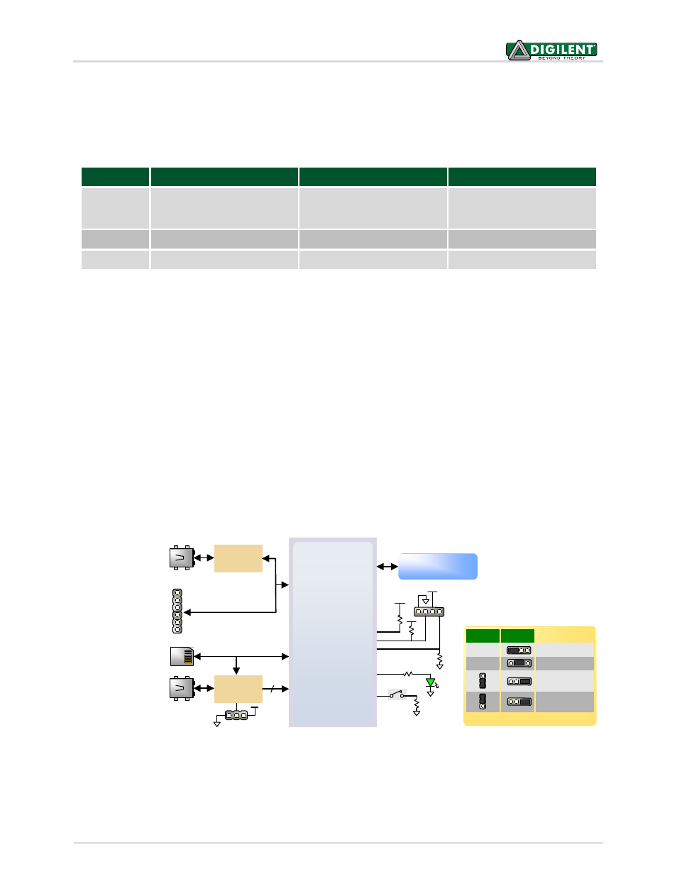
FPGA Configuration
After power-on, the Artix-7 FPGA must be configured (or programmed) before it can perform any functions. You
can configure the FPGA in one of four ways:
1. A PC can use the Digilent USB-JTAG circuitry (portJ6, labeled “PROG”) to program the FPGA any time the
power is on.
2. A file stored in the nonvolatile serial (SPI) flash device can be transferred to the FPGA using the SPI port.
3. A programming file can be transferred to the FPGA from a micro SD card.
4. A programming file can be transferred from a USB memory stick attached to the USB HID port.
Figure 3 Shows the different options available for configuring the FPGA. An on-board “mode” jumper (JP1) and a
media selection jumper (JP2) select between the programming modes.
M0
M1
JTAG
Port
USB
Controller
SPI Quad mode
Flash
1x6 JTAG
Header
SPI
Port
Micro-AB USB
Connector (J6)
USB-JTAG/UART Port
Artix-7
Done
PIC24
Type A USB Host
Connector (J5)
Serial
Prog. Port
2
6-pin JTAG
Header (J10)
Prog
Micro SD
Connector (J1)
Media Select
(JP2)
User I/O
M2
Mode (JP1)
Programming Mode
JP2
JP1
NA
SPI Flash
NA
JTAG
USB
MicroSD
The FPGA configuration data is stored in files called bitstreams that have the .bit file extension. The ISE or Vivado
software from Xilinx can create bitstreams from VHDL, Verilog, or schematic-based source files (in the ISE toolset,
EDK is used for MicroBlaze™ embedded processor-based designs).
Supply
Circuits
Device
Current (max/typical)
3.3V
FPGA I/O, USB ports, Clocks,
RAM I/O, Ethernet, SD slot,
Sensors, Flash
IC17: ADP2118
3A/0.1 to 1.5A
1.0V
FPGA Core
IC22: ADP2118
3A/ 0.2 to 1.3A
1.8V
FPGA Auxiliary and Ram
IC23: ADP2138
800mA/ 0.05 to 0.15A
Table 2. Nexys4 Power Supplies
Figure 3. Nexys4 Configuration Options