Dc voltage chart, Circuit details – Elecraft KIO2 User Manual
Page 23
23
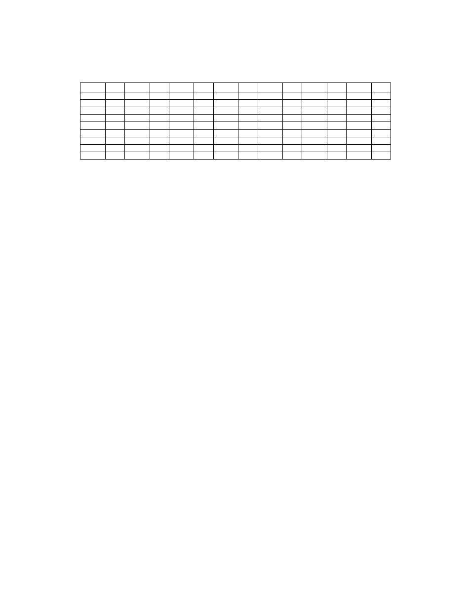
DC Voltage Chart
These measurements were made with a 14 V power supply, R2 installed, and no computer or other external
equipment connected to J1 on the KIO2. Negative voltages may vary by +/- 3V or more without affecting
performance. Voltages marked with an asterisk (*) may vary due to DMM probe loading effects.
Pin V Pin V Pin V Pin V Pin V Pin V Pin V
J1-1 0 U1-1 14 U1-10 0 J2-1 5.0 J2-10 0 Q1-G -1* D3-A -4*
J1-2 -8 U1-2 0.1
U1-11 5 J2-2 5.5
Q1-S 0* D3-C 0
J1-3 0.1 U1-3 14 U1-12 5 J2-3 5 U2
in 14 Q1-D 14 D4-A -1*
J1-4 4.5 U1-4 0.1 U1-13 4.5 J2-4 0 Out 5
D4-C 5
J1-5 0 U1-5 -8
U1-14 0 J2-5 0
D1-A -9
J1-6 5.5 U1-6 0.1 U1-15 4.5 J2-6 0
D1-C 0.1
J1-7 0 U1-7 14 U1-16 5 J2-7 4.5
D2-A -9
J1-8
14
U1-8
-9
J2-8
14
D2-C
-4*
J1-9
8
U1-9
0
J2-9
8
Circuit Details
Refer to the schematic diagram, page 24.
U1 is an RS-232 transceiver IC. It converts the 5V logic-level signals at pins 11 and 12 (RX and TX data)
to RS-232 levels, typically +/- 5 to +/- 12 VDC. Q1 is a Colpitts oscillator that drives a negative-going
detector (D2/D3). The negative voltage is filtered by C8 and supplied to U1 (pin 8) as the (-) transmit
supply voltage (Vss). L2-L4 and C3-C6 provide pi-net RF filtering. The RS-232 signal ground (J1, pin 5) is
isolated from the chassis ground (pin 1) to reduce noise pickup.
If the on-board crystal oscillator is disabled by removing R2, the negative supply voltage (U1 pin 8) is
derived from the RxD line (J1 pin 3) rather than from the oscillator. This voltage will vary depending on
the K2's serial I/O transmit duty cycle as well as the quiescent voltage supplied by the computer on RxD. If
the on-board oscillator is running (R2 installed), the negative supply voltage will be determined by either
the RxD line or the detector output (D2/D3), whichever is more negative.