Elecraft KSB2 User Manual
Page 5
5
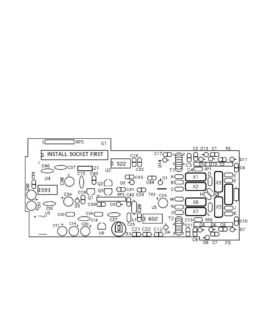
The KSB2 PC board uses close-spaced components in the crystal filter area to minimize stray signal
pickup. Some capacitors are assigned letters rather than numbers, and some components are not labeled.
Place the KSB2 PC board in front of you as shown below. At the far right end of the board, you'll find an
area with a very symmetrical layout. This area contains the SSB crystal filter and filter switching
components. In the middle of this area are a number of capacitors that are labeled only with letters (A, B,
C, D, E, F, G, H, J, K, L, M, N, P). For example, "A" corresponds to capacitor "CA" in the parts list.
Above and below the crystal filter are the filter switching components. Some of the diodes and capacitors
are not labeled on the board itself, but can be identified in the parts placement drawing below.
The only other unlabeled components are P2 and P3, which will be installed on the bottom of the board.
These are indicated in the upper-right and lower-right corners, below.
All .01 µF capacitors with 0.1" lead spacing use a special symbol with a line between the two pads to
distinguish them from small-value capacitors of the same physical size.
U3 (bottom left-hand corner) is a surface-mount device (SMD) and has been pre-installed.
Parts Placement Drawing