Ksb2 module installation – Elecraft KSB2 User Manual
Page 13
13
KSB2 Module Installation
Remove the top and bottom covers. (Do not remove the heat sink.)
Disconnect and remove the frequency counter probe.
Locate the 5-crystal CW filter on the K2 RF board (X7 through X11). If any ground wires are soldered
to the tops of these crystals, re-locate them to the sides of the crystals, about 1/4" (6 mm) up from the
surface of the PC board. Note: There are two ground pads for each of these crystals (one on either side).
For best performance, solder two wires to each crystal. (Early revisions of the K2 manual called for the use
of just one wire each, soldered to the tops of the cans, resulting in worse rejection of out-of-band signals.)
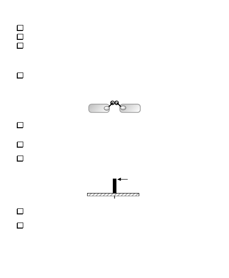
Locate the 2nd crystal filter on the RF board (X5 and X6). The ground wires on these two crystals
should be positioned approximately as shown below to maintain clearance from the SSB adapter.
(Grounding of these crystals is non-critical, so either top or side grounding will work.)
Remove jumpers W2 and W3 on the RF board (near the 5-crystal filter). It is best to de-solder these
jumpers and remove them completely rather than just cut them at both ends. If the SSB adapter must be
removed later, W2 and W3 can be re-installed, or you can insert jumpers between pins 1 and 3 of J9/J10.
Desolder and remove C167 from the RF board. C167 is located near the SSB option connector, J11.
Save C167 in case you need to remove the SSB adapter at a later date.
Install the 12-pin female connector on the RF board at J11(labeled "SSB") as shown by its outline. Do
not solder yet. The side view of J11, below, shows how it should appear once properly seated.
J11
Solder just one pin near the middle of J11. If the connector is not sitting completely flat against the RF
board, reheat this pin and press the connector down. Then solder the remaining pins of J11.
Install 3-pin female connectors on the RF board at J9 and J10, using the same technique used with J11.