Chapter 5, Sbus design examples, Sbus master design – Achronix Speedster22i sBus User Manual
Page 20: Design example, Figure 10: sbus master block diagram, Table 2: hd1000 sbus master signal definitions, Chapter 5 – sbus design examples

20
UG047, October 24, 2013
Chapter 5
– sBus Design Examples
In this chapter, you will learn the following about the sBus serial bus:
sBus Master Design
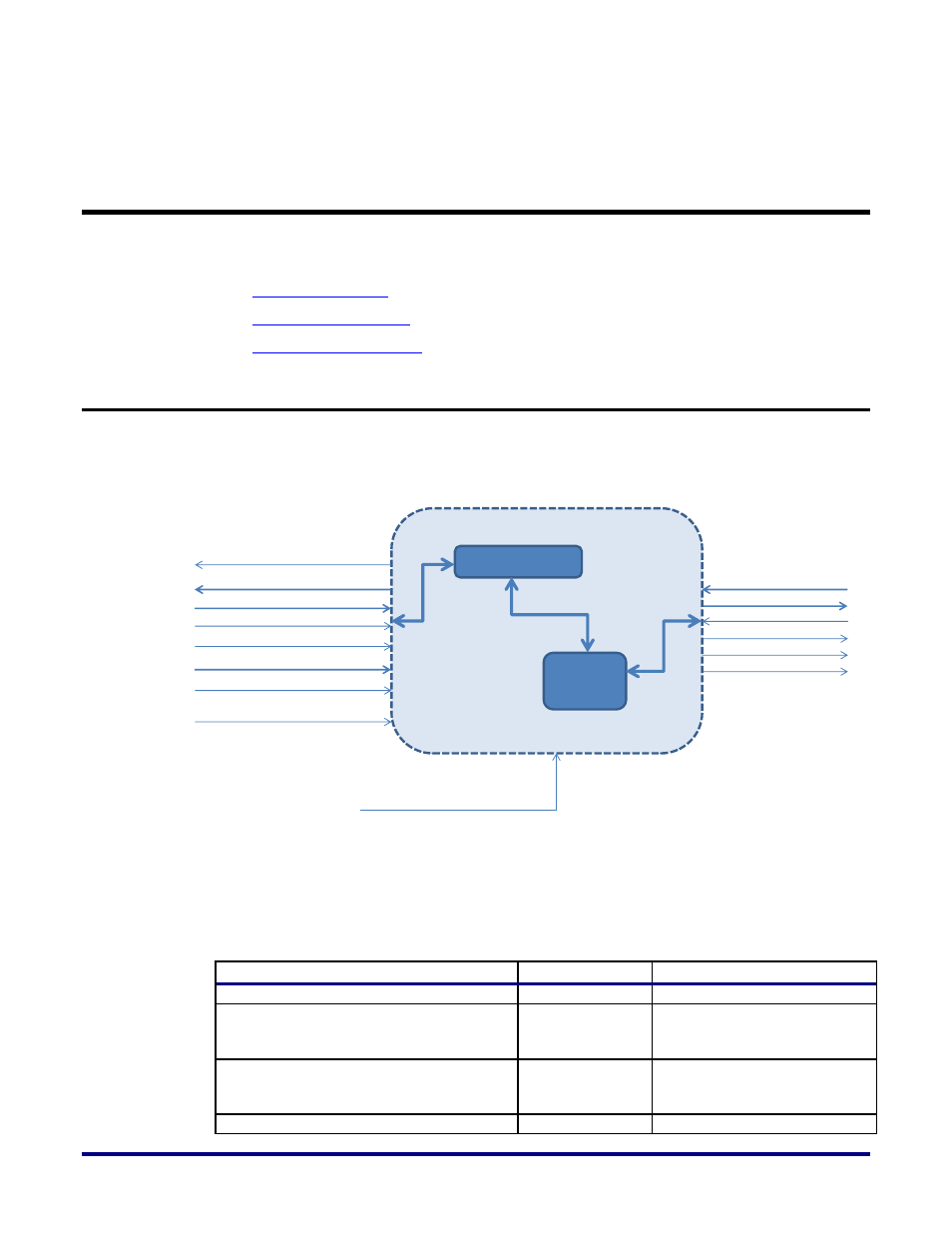
You will design and implement the sBus master in the HD1000 fabric. Figure 10 shows a
typical block diagram of a master implementation showing the interface to the parallel data
side (requester) and the sBus port (slave or hard IP) side.
Figure 10: sBus Master Block Diagram
Design Example
You will find the Verilog code for a sample master module implementation in Appendix A.
Table 2 describes the signals and their functions for this implementation.
Table 2: HD1000 sBus Master Signal Definitions
Signal
Direction
Description
i_rst_n
Input
Asynchronous reset
i_clk
Input
Reference clock for the serial
and parallel interfaces
–
sbus_clk
o_sbus_req
Output
Request signal for starting a
read or write transaction on
sBus
i_sbus_data[1:0]
Input
Input serial data of sBus
sbus_clk
reset_sbus_clk
o_sbus_req
o_sbus_data[1:0] (to slave)
i_sbus_ack
i_sbus_data[1:0] (f rom slave)
Master
Latched Parallel Data
i_reg_address [16:0]
i_sw_rst
i_reg_rw_req
i_reg_wr_data [Pbus_Data_Width - 1:0]
i_reg_write
o_reg_rd_data [Pbus_Data_Width - 1:0]
i_rst_n
i_clk
o_reg_rdwr_valid
Serializer /
Deserializer
