Achronix Speedster22i DDR User Manual
Page 26
a0
a1
a2
Valid Write commands after 5 cycles
clock
ddr_int_rd_request
ddr_int_addr[33:0]
ddr_int_busy
ddr_int_rddata_valid
ddr_int_burst_size [7:0]
...
...
...
...
4
ddr_int_rddata [287:0]
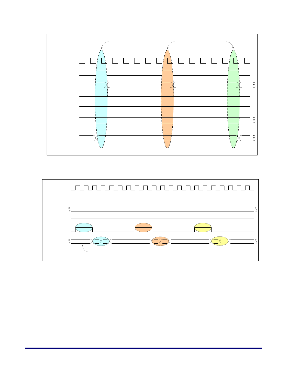
Figure 15: Read Protocol Timing Diagram (with valid read request highlighted)
Timing relationship between ddr_int_rd_request assertion and
ddr_int_wrdata_req_early assertion based on AL/CL configuration
settings refresh status and status of bank/row being assessed.
d0
d1
d0
d1
clock
ddr_int_rd_req
ddr_int_addr[33:0]
ddr_int_busy
ddr_int_rddata_valid
ddr_int_rddata [287:0]
...
...
...
...
...
...
...
...
d0
d1
...
Figure 16: Read Protocol Timing Diagram (with ddr_int_rddata_valid highlighted)
If a read request is not valid (ie. ‘ddr_int_busy’ and ‘ddr_int_rd_request’ are asserted
simultaneously), ‘ddr_int_rd_request’, ‘ddr_int_addr [33:0]’, and ‘ddr_int_burst_size [7:0]’
signal values must be latched until such time as ‘ddr_int_busy’ is de-asserted and a valid
read request (‘ddr_int_rd_request’)can be posted as shown in Figure 15. There should be 5-
clock cycle gap required for the back-to-back read request (‘ddr_int_rd_request’).
The ‘ddr_int_rd_request’ signal may remain asserted for any number (with 5-cycles apart
always) of clock periods to generate any number of follow-on read transactions (in cascaded
bursts).
The read data corresponding to a given read request is returned a deterministic number of
clock cycles after the read request. This deterministic amount of time represents the round-
26
UG031, Nov 18, 2014