Achronix Speedster22i DDR User Manual
Page 18
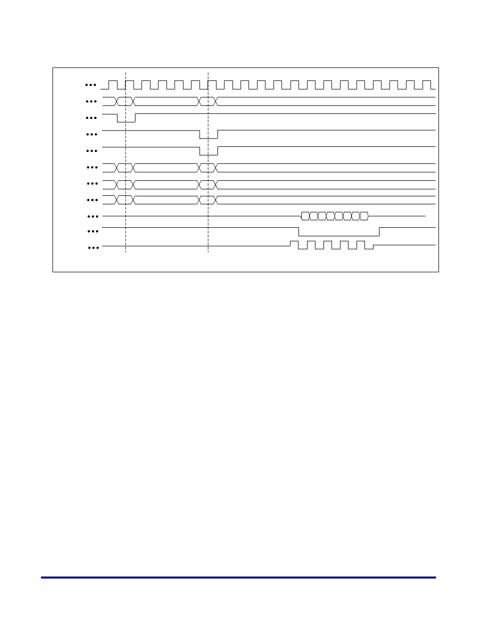
Figure 7: Write Protocol Timing Diagram (SDRAM Interface)
To request a write data transaction, the DDR driver logic (user RTL) must assert
‘ddr_int_wr_request’ along with a corresponding address (‘ddr_int_addr [33:0]’) and burst
length (‘ddr_int_burst_size’).
A valid write request (ie. one which is successfully posted to the Speedster22i DDR Controller
and propagated to the DDR Memory) is one in which ALL of the following conditions are
met:
•
‘ddr_int_wr_request’ is asserted (active high)
•
‘ddr_int_addr [33:0]’ is driven
•
‘ddr_int_burst_size [7:0]’ is driven to a valid value for the given protocol
o
8’d4 8’d252 for DDR3 (multiple of 4)
•
‘ddr_int_busy_align’ is not asserted (active high)
•
Latency of the DDR-controller provided data (ddr_int_wrdata) to the external
memory is 4-cycle.
clock
Command
sd_ras_n
sd_cas_n
Notes: For case shown, DELAY_ACTIVATE_TO_RW = 5,
CAS WRITE LATENCY =6, DELAY_ADDITIVE_DDR3_LATENCY=0
d0r
d0f
d1r
d1f
d2r
d2f
d3r
d3f
ACT
WR
sd_we_n
sd_a
sd_ba
sd_cs_n
sd_dq
sd_dm
sd_dqs
ROW
COL
BANK
BANK
CHIP
CHIP
18
UG031, Nov 18, 2014