Achronix Speedster22i DDR User Manual
Page 16
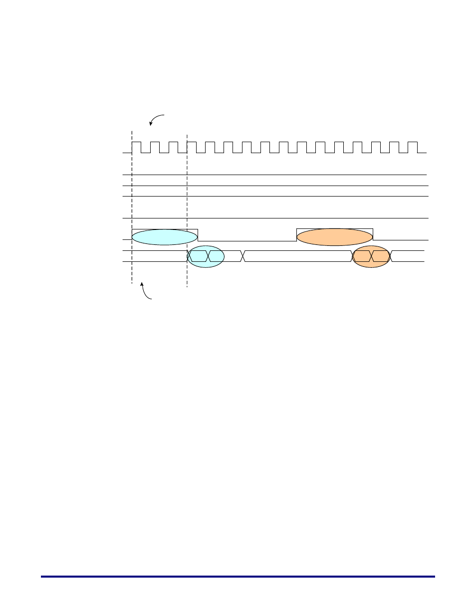
The following timing diagram illustrates a single write command of burst length 4. The
signals shown in the following diagrams are ports at the (‘ddr3_xSIZE
1
_LOCATION
2
’.
Where 1: SIZE = 72, 64, 32, 16, 8 and 2: LOCATION=EN, EC, ES, WN, WC, WS).
Figure 5: Internal Interface Write Protocol Timing Diagram
This 2-cycles delay between the ‘ddr_int_wrdata_req_early_align’ and ‘ddr_int_wrdata
[287:0]’ is optional. This is implemented using a parameter ‘addrcmd_delay’ value
setting to “4’h9”. This extra cycle provides an advantage to the user to latch the data to be
written to the PHY. This implementation is optional to the user. If the user wants to use
1-cycle delay between ‘ddr_int_wrdata_req_early_align’ and ‘ddr_int_wrdata [287:0]’, in
this case let keep the default value of the parameter ‘addrcmd_delay’. The default values
for this parameter ‘addrcmd_delay’ is “4’h8”. The user needs to be very careful about
their implementation while using Achronix DDR-controller implementing 1-cycle delay
implementation for latching the write-data to be written to PHY. For the 2-cycle delay,
the user has enough time to latch the data.
The diagram above shows the signals between the FPGA fabric core and DDR controller.
(‘ddr_int_wrdata_req_early_align’) signal is 3 cycles earlier then (‘ddr_int_wrdata_req’)
signal. The user can use ‘ddr_int_wrdata_req_early_align’ signal to be ready to write the
data and at the assertion of ‘ddr_int_wrdata_req’ signal to drive user data on
‘ddr_int_wrdata’.
clk_div2
ddr_int_wr_request
ddr_int_addr[33:0]
ddr_int_busy
d0
d1
d0
d1
ddr_int_wrdata
[143:0]
Timing relationship between ddr_int_wr_request assertion
and ddr_int_wrdata_req_early assertion based on AL/CL
configuration settings, refresh status and status on bank/
row being accessed
ddr_int_wrdata_req_early
Present data 3-cycles after
ddr_int_wrdata_req_early is
asserted
16
UG031, Nov 18, 2014