External (off-chip) interface, Parameters – Achronix Speedster22i DDR User Manual
Page 11
External (off-chip) Interface
The External DDR interface signals (off-chip) from the DDR PHY to the external memory devices are
shown in Table 2 below.
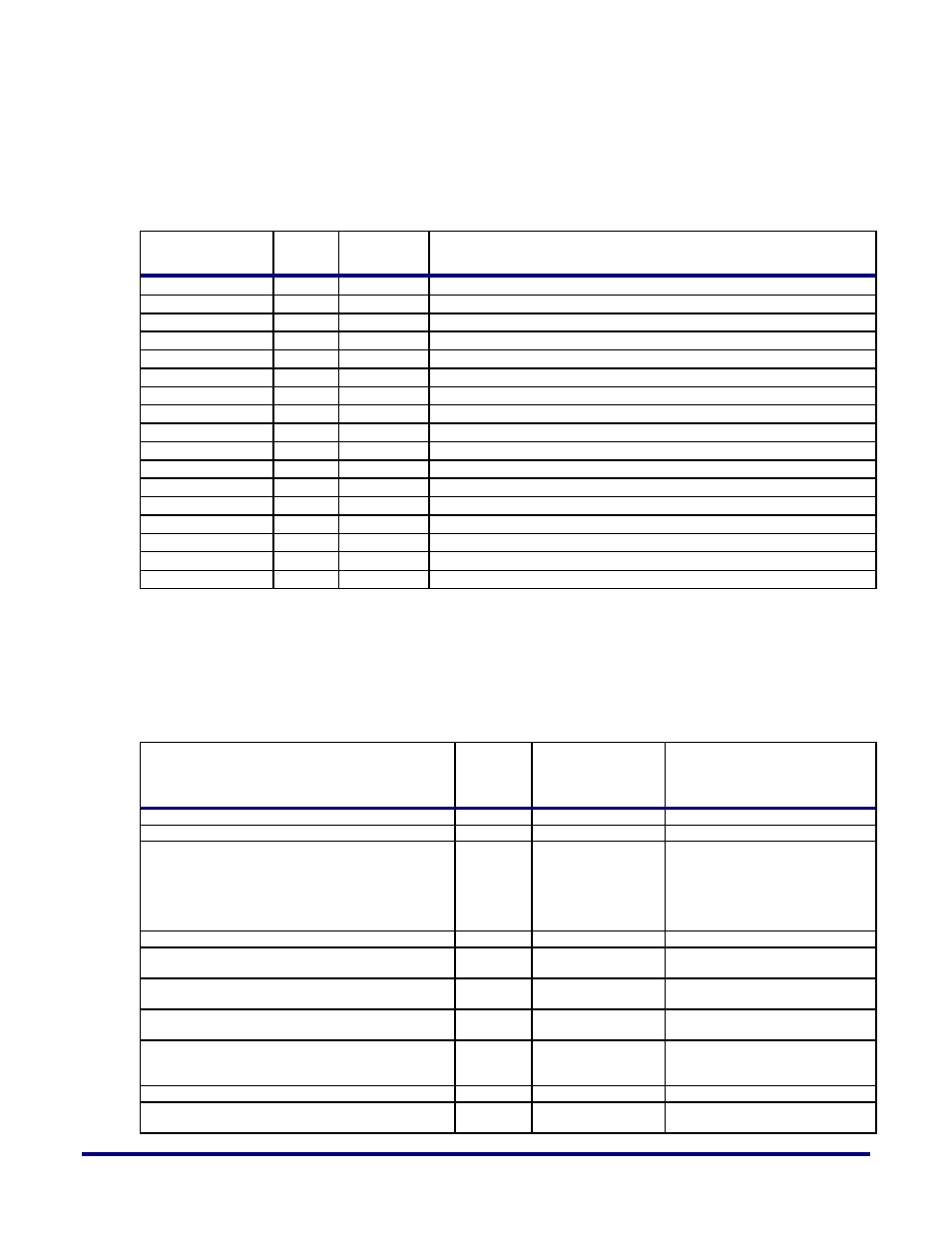
Signal Name
Bus
Width
Direction Description
sd_clk_p
4
Output
SDRAM clock signal
sd_clk_n
4
Output
SDRAM clock signal
sd_cke
4
Output
SDRAM clock enable control signal
sd_odt
4
Output
SDRAM on die termination control signal
sd_ras_n
1
Output
SDRAM RAS control signal
sd_cas_n
1
Output
SDRAM CAS control signal
sd_we_n
1
Output
SDRAM write enable control signal
sd_reset_n
1
Output
SDRAM reset signal
sd_a
16
Output
SDRAM address bus
sd_ba
3
Output
SDRAM bank select
sd_cs_n
4
Output
SDRAM chip select
sd_dm
9
Output
SDRAM data mask
sd_dummy
9
Output
Internal use only. Leave unconnected
sd_dq
72
Inout
SDRAM data bus
sd_dqsn
9
Inout
SDRAM DQS bus, which is used to clock DQ bus
sd_dqsp
9
Inout
SDRAM DQS bus, which is used to clock DQ bus
Table-2: PHY/DDR controller to memory interface signals
Parameters
Parameters that can be set for both the DDR controller and PHY are shown in Table 3 below.
Parameter
Default
Value
(hex)
Valid Values
Description
DSIZE
72
Multiples of 8 from 8-72 Local side data width
NUM_CLK_OUTS
3
1 to 4
Number of clock outputs
CONTROLLER_REFRESH_EN
1'h1
0-1
Enable controller initiated refreshes.
0: Embedded DDR Controller
automatically handles cyclic
autorefreshing of memory.
1: User manually overrides autorefresh
control of memory.
DELAY_ACTIVATE_TO_PRECHARGE
5'h14
4-30 clock cycles
Minimum ACTIVE to PRECHARGE
DELAY_ACTIVATE_TO_RW
4'h7
2-12 clock cycles
Minimum time between ACTIVATE
and READ/WRITE
DELAY_ACTIVATE_TO_ACTIVATE_DIFF_BANK
3'h4
2-6 clock cycles
Minimum time between ACTIVATE to
ACTIVATE in different banks
DELAY_PRECHARGE_TO_ACTIVATE
4'h7
1-12 clock cycles
Minimum PRECHARGE to
ACTIVATE.
DELAY_ACTIVATE_TO_ACTIVATE_SAME_BANK
6'h20
5-42 clock cycles
Minimum ACTIVATE to
ACTIVATE/AUTO-REFRESH in same
bank
BANK_ACTIVATE_PERIOD
6'h20
7-32 clock cycles
Four bank activate period
DELAY_AUTO_REFRESH_TO_ACTIVATE_SAME_BANK
9'h03B
6-511 clock cylces
Minimum AUTO-REFRESH to
ACTIVATE/AUTO-REFRESH in same
UG031, Nov 18, 2014
11