Achronix Speedster22i DDR User Manual
Page 20
...
...
Timing relationship between ddr_int_wr_request assertion and
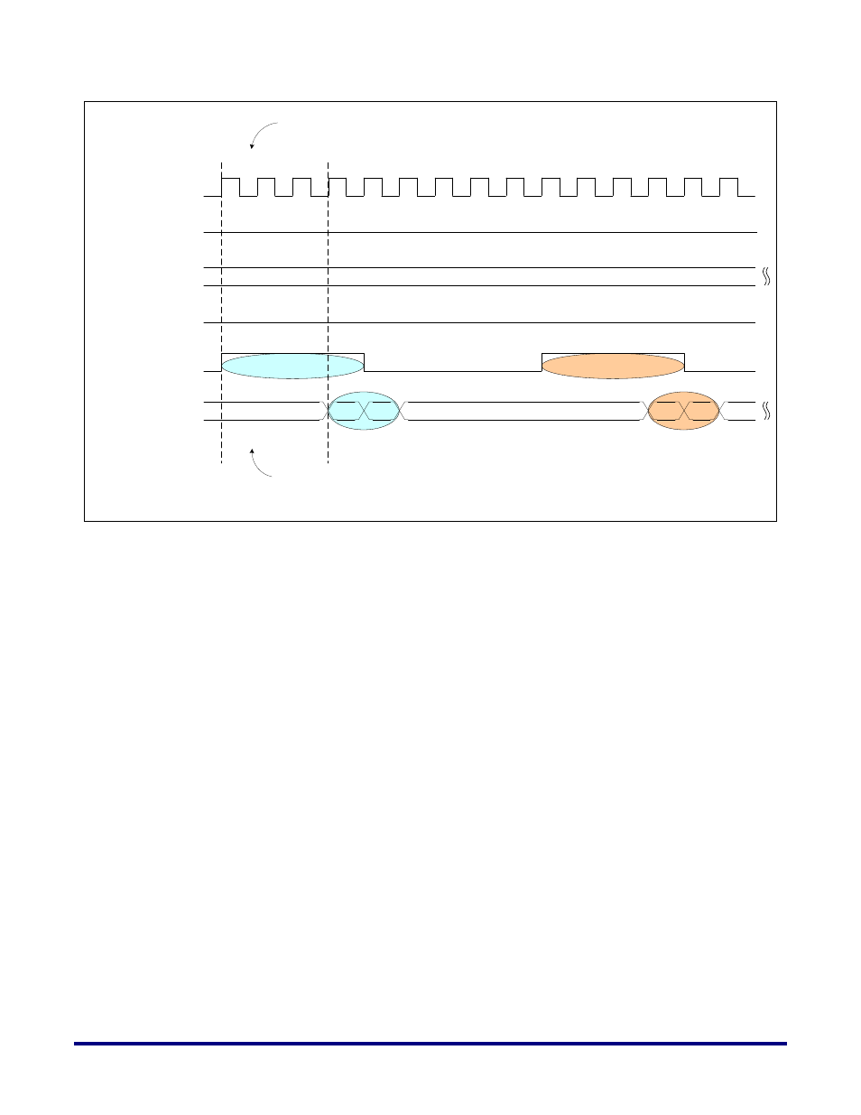
ddr_int_wrdata_req_early assertion based on AL/CL
configuration settings, refresh status and status on bank/row
being accessed
...
ddr_int_addr[33:0]
ddr_int_wr_request
clk_div2
ddr_int_busy
ddr_int_wrdata_req_early
ddr_int_wrdata[143:0]
d0
d1
d0
d1
...
Present data 3-cycles after
ddr_int_wrdata_req_early is
asserted
Figure 9: Write Protocol Timing Diagram (ddr_int_wrdata_req corresponding to respective writes highlighted)
If a write request is not valid (ie. ‘ddr_int_busy’ and ‘ddr_int_wr_request’ are asserted
simultaneously), ‘ddr_int_wr_request’, ddr_int_addr [33:0]’, and ‘ddr_int_burst_size [7:0]’
signal values must be latched until ‘ddr_int_busy’ is de-asserted and a valid write request
(‘ddr_int_wr_request’)can be posted as shown in Figure 8. There should be 5-cycles delay
between the back-to-back ‘ddr_int_wr_request’ signal as shown in Figure 8. Corresponding
‘ddr_int_wrdata_req’ and ‘ddr_int_wrdata’ timing is shown in Figure 9.
The ‘ddr_int_wr_request’ signal may remain asserted for any number (with 5-cycles apart
always) to generate any number of follow-on writes transactions (in cascaded bursts).
The data request (‘ddr_int_wrdata_req’) signal will be asserted two cycles prior to when the
DDR driver logic (user RTL) must present data at the ‘ddr_int_wrdata’ bus and mask
information at the ‘ddr_int_writedata_mask’ bus.
The Speedster22i DDR Controller will ensure that the ‘ddr_int_wrdata_req_early’ signal is
asserted for the correct number of cycles (based on the ‘ddr_int_burst_size’ value specified
for the corresponding write request) as well as at the correct time (in accordance with DDR
latency requirements based on user-specified values of AL and CL parameters in the case of
DDR/DDR2, or AL and CWL parameters in the case of DDR3).
The burst length (‘ddr_int_burst_size’) corresponding to a single given write request must be
set to a valid value based on the given DDR protocol. For DDR3 has a range of 8’d4 to
8’d252. Note that the ‘ddr_int_burst_size’ value translates directly to the number of cycles
for which ‘ddr_int_wrdata_req’ is asserted.
While bank and row addresses are derived directly from the address provided by the user
(ie. DDR driver logic) for a given write request, the column address is incremented
automatically within the Speedster22i DDR Controller for a given burst, starting with the
20
UG031, Nov 18, 2014