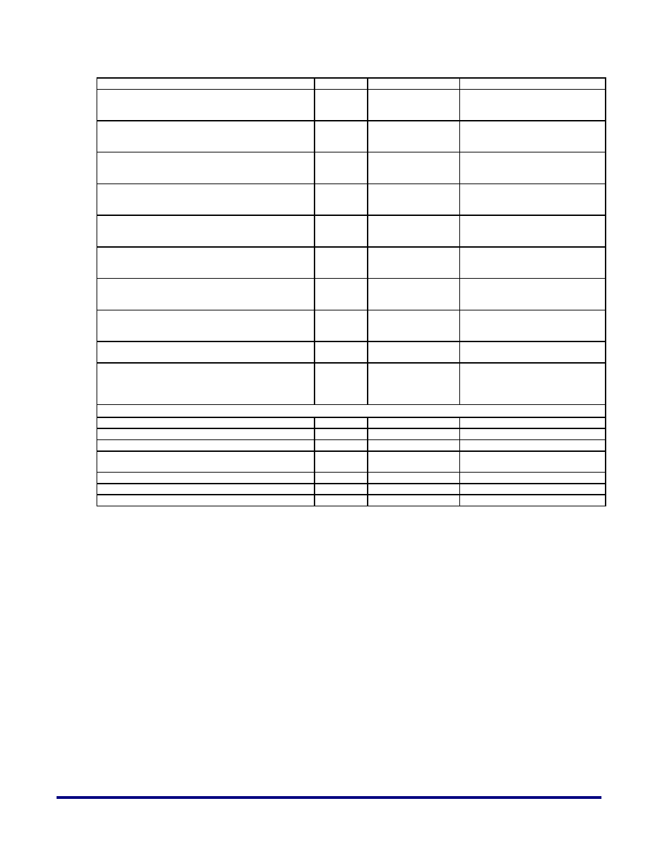
Table-3: parameter values of the ddr controller – Achronix Speedster22i DDR User Manual
Page 13

is enabled when set to 1
ODT_WRITE_CS0
8'h01
Each bank contains 8
bits, one per DQ. ODT
is enabled when set to 1
On die termination selection for writes
on cs0
ODT_WRITE_CS1
8'h02
Each bank contains 8
bits, one per DQ. ODT
is enabled when set to 1
On die termination selection for writes
on cs1
ODT_WRITE_CS2
8'h04
Each bank contains 8
bits, one per DQ. ODT
is enabled when set to 1
On die termination selection for writes
on cs2
ODT_WRITE_CS3
8'h08
Each bank contains 8
bits, one per DQ. ODT
is enabled when set to 1
On die termination selection for writes
on cs3
ODT_WRITE_CS4
8’h10
Each bank contains 8
bits, one per DQ. ODT
is enabled when set to 1
On die termination selection for writes
on cs4
ODT_WRITE_CS5
8’h20
Each bank contains 8
bits, one per DQ. ODT
is enabled when set to 1
On die termination selection for writes
on cs5
ODT_WRITE_CS6
8’h40
Each bank contains 8
bits, one per DQ. ODT
is enabled when set to 1
On die termination selection for writes
on cs6
ODT_WRITE_CS7
8’h80
Each bank contains 8
bits, one per DQ. ODT
is enabled when set to 1
On die termination selection for writes
on cs7
READ_EN_DELAY_LANE
3’h5
0-5
Adjusts the delay of the read data out of
the PHY
BYPASS_TXRX_SD
0
0 or 1
0 1X clock mode. Core run at same
speed as controller
1 2X clock mode. Core run at half the
speed of controller.
If no soft write leveling or read leveling is used, then use these parameters:
BYTE_LANE*_DLL_ADJ_DQ (2)
6’h4
DQ Slave adjust for Byte Lane *
BYTE_LANE*_DLL_ADJ_DQS (2)
6’h16
DQS Slave adjust for Byte Lane *
BYTE_LANE*_DLL_ADJ_DP (2)
6’h6
DP Slave adjust for Byte Lane *
BYTE_LANE*_WR_LVL_DQ_SELECT (2)
4’b0000
Which DQ bit is used for write leveling
*
BYTE_LANE_DLL_MADJ
8’h2a
Master adjust
BYTE_LANE_DLL_DQSX9_CLK_ADJ
8’h3f
Slave adjust for DQSX9
BYTE_LANE_CAC_DLL_ADJ_DQSN
6’h17
Slave adjust for address bytes lanes
Table-3: Parameter values of the DDR controller
Notes on Table 3
:
1.
These parameters are available for all byte lanes. For example if we have 64 DQ bits that will be 8 byte
lane. So these parameters are available for all 8 lanes, replace the * with each byte number.
UG031, Nov 18, 2014
13
