Codec interface, Ssi2 interface, Synchronous serial interface – Cirrus Logic EP7311 User Manual
Page 8: Lcd controller
8
Copyright Cirrus Logic, Inc. 2011
(All Rights Reserved)
DS506F2
EP7311
High-Performance, Low-Power System on Chip
CODEC Interface
The EP7311 includes an interface to telephony-type CODECs
for easy integration into voice-over-IP and other voice
communications systems. The CODEC interface is
multiplexed to the same pins as the MCP and SSI2.
Note:
See
for information on pin
multiplexes.
SSI2 Interface
An additional SPI/Microwire1-compatible interface is
available for both master and slave mode communications. The
SSI2 unit shares the same pins as the MCP and CODEC
interfaces through a multiplexer.
•
Synchronous clock speeds of up to 512 kHz
•
Separate 16 entry TX and RX half-word wide FIFOs
•
Half empty/full interrupts for FIFOs
•
Separate RX and TX frame sync signals for asymmetric
traffic
Note:
See
for information on pin
multiplexes.
Synchronous Serial Interface
•
ADC (SSI) Interface: Master mode only; SPI and
Microwire1-compatible (128 kbps operation)
•
Selectable serial clock polarity
LCD Controller
A DMA address generator is provided that fetches video
display data for the LCD controller from memory. The display
frame buffer start address is programmable, allowing the LCD
frame buffer to be in SDRAM, internal SRAM or external
SRAM.
•
Interfaces directly to a single-scan panel monochrome STN
LCD
•
Interfaces to a single-scan panel color STN LCD with
minimal external glue logic
•
Panel width size is programmable from 32 to 1024 pixels in
16-pixel increments
•
Video frame buffer size programmable up to
128 KB
•
Bits per pixel of 1, 2, or 4 bits
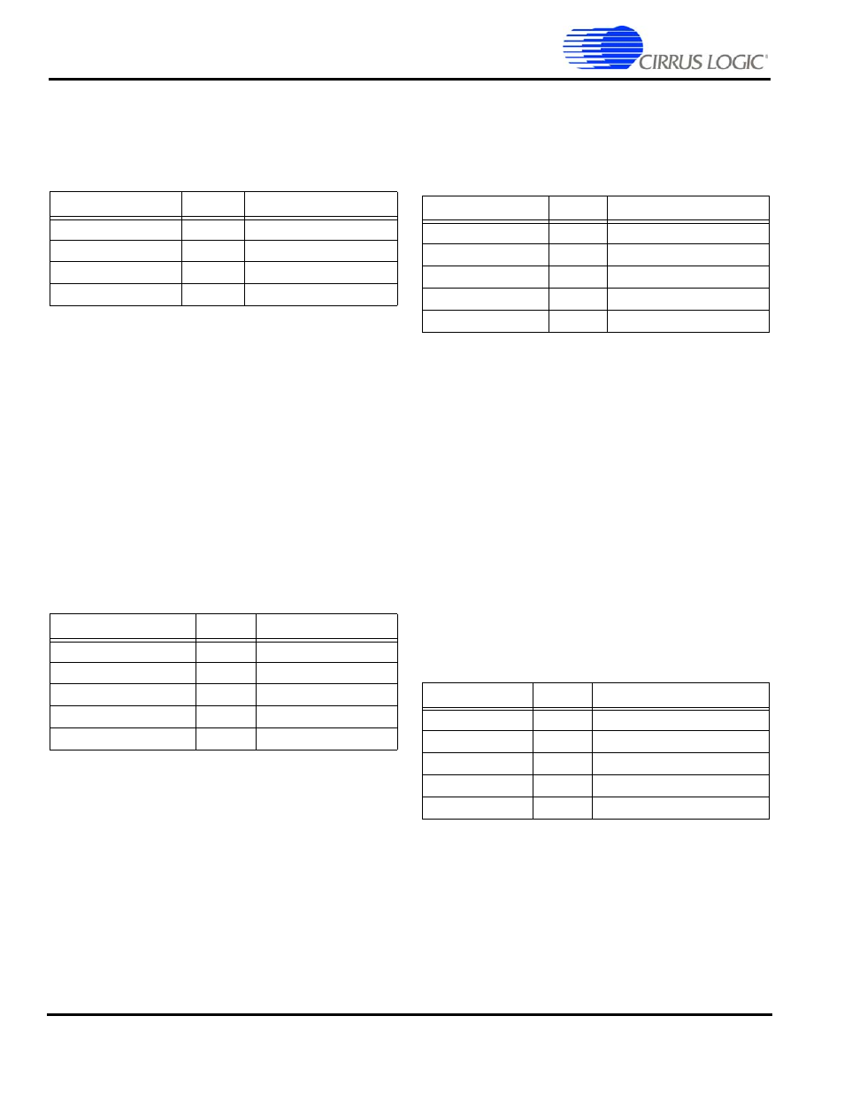
Pin Mnemonic
I/O
Pin Description
PCMCLK
O
Serial bit clock
PCMOUT
O
Serial data out
PCMIN
I
Serial data in
PCMSYNC
O
Frame sync
Table F. CODEC Interface Pin Assignments
Pin Mnemonic
I/O
Pin Description
SSICLK
I/O
Serial bit clock
SSITXDA
O
Serial data out
SSIRXDA
I
Serial data in
SSITXFR
I/O
Transmit frame sync
SSIRXFR
I/O
Receive frame sync
Table G. SSI2 Interface Pin Assignments
Pin Mnemonic
I/O
Pin Description
ADCLK
O
SSI1 ADC serial clock
ADCIN
I
SSI1 ADC serial input
ADCOUT
O
SSI1 ADC serial output
nADCCS
O
SSI1 ADC chip select
SMPCLK
O
SSI1 ADC sample clock
Table H. Serial Interface Pin Assignments
Pin Mnemonic
I/O
Pin Description
CL1
O
LCD line clock
CL2
O
LCD pixel clock out
DD[3:0]
O
LCD serial display data bus
FRM
O
LCD frame synchronization pulse
M
O
LCD AC bias drive
Table I. LCD Interface Pin Assignments