Ds506f2 – Cirrus Logic EP7311 User Manual
Page 33
DS506F2
Copyright Cirrus Logic, Inc. 2011
(All Rights Reserved)
33
EP7311
High-Performance, Low-Power System on Chip
F7
SDCKE
O
SDRAM clock enable output
F8
DD[3]
O
LCD serial display data
F9
A[1]
O
System byte address
F10
D[6]
I/O
Data I/O
F11
VSSRTC
RTC ground Real time clock ground
F12
BATOK
I
Battery ok input
F13
nBATCHG
I
Battery changed sense input
F14
VSSIO
Pad ground
I/O ground
F15
D[11]
I/O
Data I/O
F16
VDDIO
Pad power
Digital I/O power, 3.3V
G1
PB[1]
I
GPIO port B
G2
VDDIO
Pad power
Digital I/O power, 3.3V
G3
TDO
O
JTAG data out
G4
PB[4]
I
GPIO port B
G5
PB[6]
I
GPIO port B
G6
VSSRTC
Core ground Real time clock ground
G7
VSSRTC
RTC ground Real time clock ground
G8
DD[0]
O
LCD serial display data
G9
D[3]
I/O
Data I/O
G10
VSSRTC
RTC ground Real time clock ground
G11
A[7]
O
System byte address
G12
A[8]
O
System byte address
G13
A[9]
O
System byte address
G14
VSSIO
Pad ground
I/O ground
G15
D[12]
I/O
Data I/O
G16
D[13]
I/O
Data I/O
H1
PA[7]
I
GPIO port A
H2
PA[5]
I
GPIO port A
H3
VSSIO
Pad ground
I/O ground
H4
PA[4]
I
GPIO port A
H5
PA[6]
I
GPIO port A
H6
PB[0]
I
GPIO port B
H7
PB[2]
I
GPIO port B
H8
VSSRTC
RTC ground Real time clock ground
H9
VSSRTC
RTC ground Real time clock ground
H10
A[10]
O
System byte address
H11
A[11]
O
System byte address
H12
A[12]
O
System byte address
H13
A[13]/DRA[14]
O
System byte address / SDRAM address
H14
VSSIO
Pad ground
I/O ground
H15
D[14]
I/O
Data I/O
H16
D[15]
I/O
Data I/O
J1
PA[3]
I
GPIO port A
J2
PA[1]
I
GPIO port A
J3
VSSIO
Pad ground
I/O ground
J4
PA[2]
I
GPIO port A
J5
PA[0]
I
GPIO port A
J6
TXD[1]
O
UART 1 transmit data out
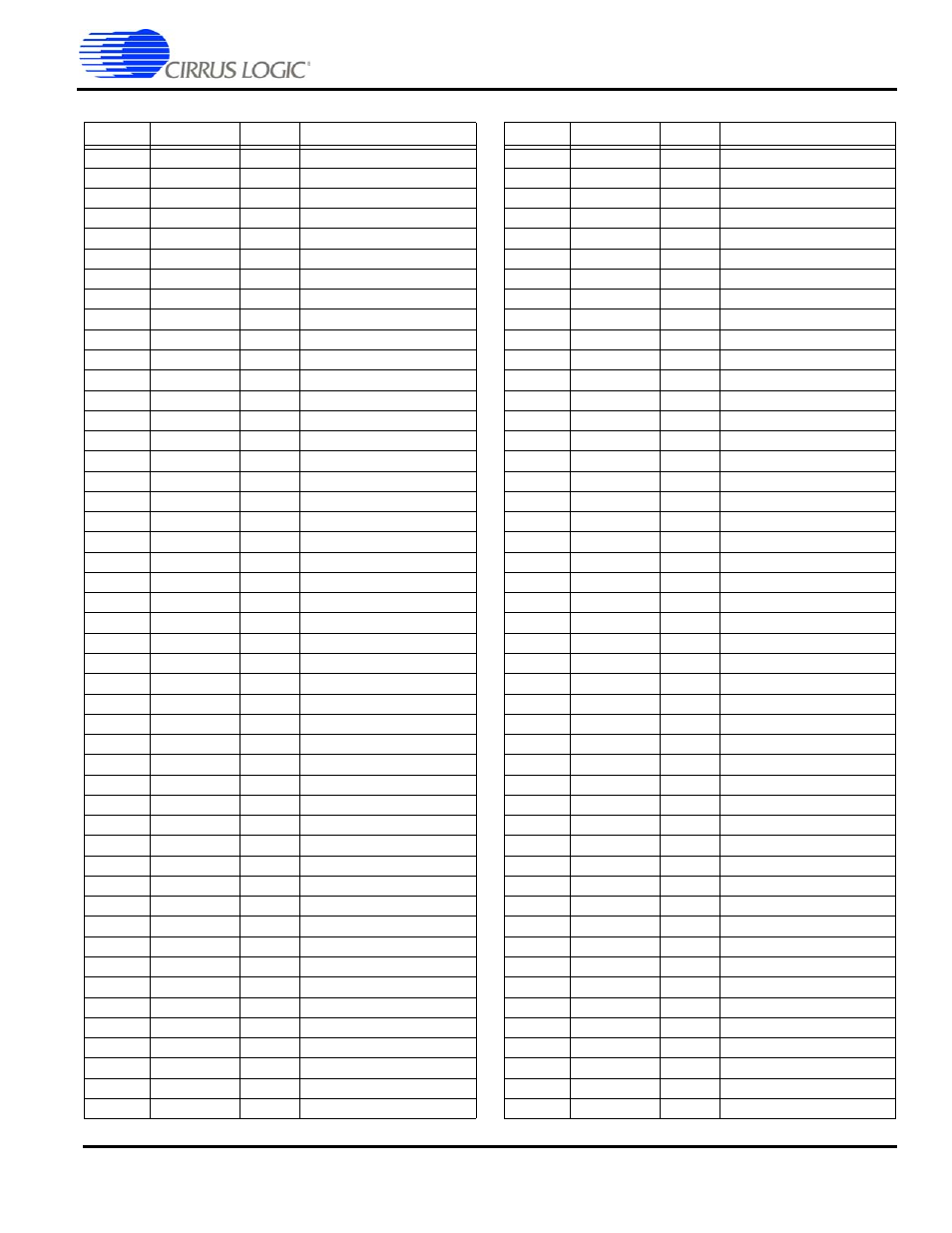
Table T. 256-Ball PBGA Ball Listing (Continued)
Ball Location
Name
Type
Description
J7
CTS
I
UART 1 clear to send input
J8
VSSRTC
RTC ground Real time clock ground
J9
VSSRTC
RTC ground Real time clock ground
J10
A[17]/DRA[10]
O
System byte address / SDRAM address
J11
A[16]/DRA[11]
O
System byte address / SDRAM address
J12
A[15]/DRA[12]
O
System byte address / SDRAM address
J13
A[14]/DRA[13]
O
System byte address / SDRAM address
J14
nTRST
I
JTAG async reset input
J15
D[16]
I/O
Data I/O
J16
D[17]
I/O
Data I/O
K1
LEDDRV
O
IR LED drivet
K2
PHDIN
I
Photodiode input
K3
VSSIO
Pad ground
I/O ground
K4
DCD
I
UART 1 data carrier detect
K5
nTEST[1]
I
Test mode select input
K6
EINT[3]
I
External interrupt
K7
VSSRTC
RTC ground Real time clock ground
K8
ADCIN
I
SSI1 ADC serial input
K9
COL[4]
O
Keyboard scanner column drive
K10
TCLK
I
JTAG clock
K11
D[20]
I/O
Data I/O
K12
D[19]
I/O
Data I/O
K13
D[18]
I/O
Data I/O
K14
VSSIO
Pad ground
I/O ground
K15
VDDIO
Pad power
Digital I/O power, 3.3V
K16
VDDIO
Pad power
Digital I/O power, 3.3V
L1
RXD[1]
I
UART 1 receive data input
L2
DSR
I
UART 1 data set ready input
L3
VDDIO
Pad power
Digital I/O power, 3.3V
L4
nEINT[1]
I
External interrupt input
L5
PE[2]/CLKSEL
I
GPIO port E / clock input mode select
L6
VSSRTC
RTC ground Real time clock ground
L7
PD[0]/LEDFLSH
I/O
GPIO port D / LED blinker output
L8
VSSRTC
Core ground Real time clock ground
L9
COL[6]
O
Keyboard scanner column drive
L10
D[31]
I/O
Data I/O
L11
VSSRTC
RTC ground Real time clock ground
L12
A[22]/DRA[5]
O
System byte address / SDRAM address
L13
A[21]/DRA[6]
O
System byte address / SDRAM address
L14
VSSIO
Pad ground
I/O ground
L15
A[18]/DRA[9]
O
System byte address / SDRAM address
L16
A[19]/DRA[8]
O
System byte address / SDRAM address
M1
nTEST[0]
I
Test mode select input
M2
nEINT[2]
I
External interrupt input
M3
VDDIO
Pad power
Digital I/O power, 3.3V
M4
PE[0]/BOOTSEL[0]
I
GPIO port E / Boot mode select
M5
TMS
I
JTAG mode select
M6
VDDIO
Pad power
Digital I/O power, 3.3V
Table T. 256-Ball PBGA Ball Listing (Continued)
Ball Location
Name
Type
Description