Ball pbga ball listing, Table t. 256-ball pbga ball listing, The list is ordered by ball location – Cirrus Logic EP7311 User Manual
Page 32
32
Copyright Cirrus Logic, Inc. 2011
(All Rights Reserved)
DS506F2
EP7311
High-Performance, Low-Power System on Chip
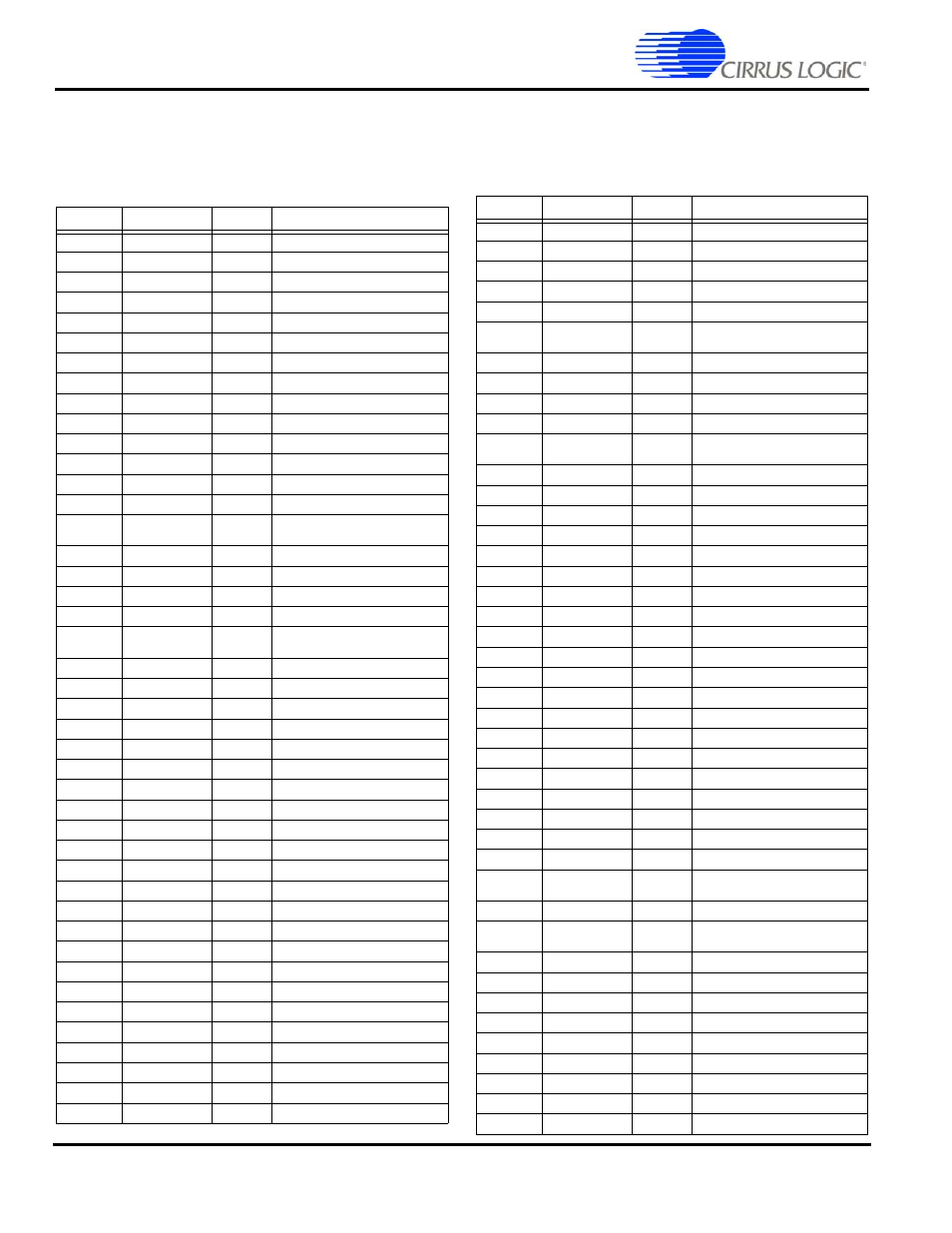
256-Ball PBGA Ball Listing
The list is ordered by ball location.
Table T. 256-Ball PBGA Ball Listing
Ball Location
Name
Type
Description
A1
VDDIO
Pad power
Digital I/O power, 3.3V
A2
nCS[4]
O
Chip select out
A3
nCS[1]
O
Chip select out
A4
SDCLK
O
SDRAM clock out
A5
SDQM[3]
O
SDRAM byte lane mask
A6
DD[1]
O
LCD serial display data
A7
M
O
LCD AC bias drive
A8
VDDIO
Pad power
Digital I/O power, 3.3V
A9
D[0]
I/O
Data I/O
A10
D[2]
I/O
Data I/O
A11
A[3]
O
System byte address
A12
VDDIO
Pad power
Digital I/O power, 3.3V
A13
A[6]
O
System byte address
A14
MOSCOUT
O
Main oscillator out
A15
VDDOSC
Oscillator
power
Oscillator power in, 2.5V
A16
VSSIO
Pad ground
I/O ground
B1
nCS[5]
O
Chip select out
B2
VDDIO
Pad power
I/O ground
B3
nCS[3]
O
Chip select out
B4 nMOE/nSDCAS
O
ROM, expansion OP enable/SDRAM
CAS control signal
B5
VDDIO
Pad power
Digital I/O power, 3.3V
B6
nSDCS[1]
O
SDRAM chip select out
B7
DD[2]
O
LCD serial display data
B8
CL[1]
O
LCD line clock
B9
VDDCORE
Core power
Digital core power, 2.5V
B10
D[1]
I/O
Data I/O
B11
A[2]
O
System byte address
B12
A[4]
O
System byte address
B13
A[5]
O
System byte address
B14
WAKEUP
I
System wake up input
B15
VDDIO
Pad power
Digital I/O power, 3.3V
B16
nURESET
I
User reset input
C1
VDDIO
Pad power
Digital I/O power, 3.3V
C2
EXPCLK
I
Expansion clock input
C3
VSSIO
Pad ground
I/O ground
C4
VDDIO
Pad power
Digital I/O power, 3.3V
C5
VSSIO
Pad ground
I/O ground
C6
VSSIO
Pad ground
I/O ground
C7
VSSIO
Pad ground
I/O ground
C8
VDDIO
Pad power
Digital I/O power, 3.3V
C9
VSSIO
Pad ground
I/O ground
C10
VSSIO
Pad ground
I/O ground
C11
VSSIO
Pad ground
I/O ground
C12
VDDIO
Pad power
Digital I/O power, 3.3V
C13
VSSIO
Pad ground
I/O ground
C14
VSSIO
Pad ground
I/O ground
C15
nPOR
I
Power-on reset input
C16
nEXTPWR
I
External power supply sense input
D1 WRITE/nSDRAS
O
Transfer direction / SDRAM RAS signal
output
D2
EXPRDY
I
Expansion port ready input
D3
VSSIO
Pad ground
I/O ground
D4
VDDIO
Pad power
Digital I/O power, 3.3V
D5
nCS[2]
O
Chip select out
D6 nMWE/nSDWE
O
ROM, expansion write enable/ SDRAM
write enable control signal
D7
nSDCS[0]
O
SDRAM chip select out
D8
CL[2]
O
LCD pixel clock out
D9
VSSRTC
Core ground Real time clock ground
D10
D[4]
I/O
Data I/O
D11
nPWRFL
I
Power fail sense input
D12
MOSCIN
I
Main oscillator input
D13
VDDIO
Pad power
Digital I/O power, 3.3V
D14
VSSIO
Pad ground
I/O ground
D15
D[7]
I/O
Data I/O
D16
D[8]
I/O
Data I/O
E1
RXD[2]
I
UART 2 receive data input
E2
PB[7]
I
GPIO port B
E3
TDI
I
JTAG data input
E4
WORD
O
Word access select output
E5
VSSIO
Pad ground
I/O ground
E6
nCS[0]
O
Chip select out
E7
SDQM[2]
O
SDRAM byte lane mask
E8
FRM
O
LCD frame synchronization pulse
E9
A[0]
O
System byte address
E10
D[5]
I/O
Data I/O
E11
VSSOSC
Oscillator
ground
PLL ground
E12
VSSIO
Pad ground
I/O ground
E13
nMEDCHG/nBROM
I
Media change interrupt input / internal
ROM boot enable
E14
VDDIO
Pad power
Digital I/O power, 3.3V
E15
D[9]
I/O
Data I/O
E16
D[10]
I/O
Data I/O
F1
PB[5]
I
GPIO port B
F2
PB[3]
I
GPIO port B
F3
VSSIO
Pad ground
I/O ground
F4
TXD[2]
O
UART 2 transmit data output
F5
RUN/CLKEN
O
Run output / clock enable output
F6
VSSIO
Pad ground
I/O ground
Table T. 256-Ball PBGA Ball Listing (Continued)
Ball Location
Name
Type
Description