Digital audio capability, Multimedia codec port (mcp) – Cirrus Logic EP7311 User Manual
Page 7
DS506F2
Copyright Cirrus Logic, Inc. 2011
(All Rights Reserved)
7
EP7311
High-Performance, Low-Power System on Chip
The second is the programmable 16- or 32-bit-wide SDRAM
interface that allows direct connection of up to two banks of
SDRAM, totaling 512 Mb. To assure the lowest possible power
consumption, the EP7311 supports self-refresh SDRAMs,
which are placed in a low-power state by the device when it
enters the low-power Standby State.
Note:
1. Pins A[27:13] map to DRA[0:14] respectively.
(i.e. A[27}/DRA[0}, A[26}/DRA[1], etc.) This is to
balance the load for large memory systems.
2. Pins are multiplexed. See
more information.
Digital Audio Capability
The EP7311 uses its powerful 32-bit RISC processing engine
to implement audio decompression algorithms in software. The
nature of the on-board RISC processor, and the availability of
efficient C-compilers and other software development tools,
ensures that a wide range of audio decompression algorithms
can easily be ported to and run on the EP7311
Universal Asynchronous
Receiver/Transmitters (UARTs)
The EP7311 includes two 16550-type UARTs for RS-232
serial communications, both of which have two 16-byte FIFOs
for receiving and transmitting data. The UARTs support bit
rates up to 115.2 kbps. An IrDA SIR protocol encoder/decoder
can be optionally switched into the RX/TX signals to/from
UART 1 to enable these signals to drive an infrared
communication interface directly.
Multimedia Codec Port (MCP)
The Multimedia Codec Port provides access to an audio codec,
a telecom codec, a touchscreen interface, four general purpose
analog-to-digital converter inputs, and ten programmable
digital I/O lines.
Note:
See
for information on pin
multiplexes.
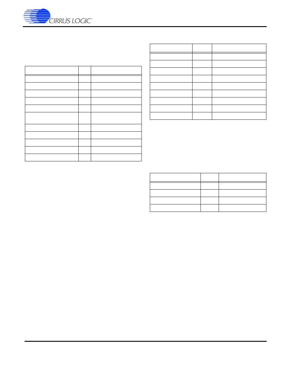
Pin Mnemonic
I/O
Pin Description
SDCLK
O
SDRAM clock output
SDCKE
O
SDRAM clock enable output
nSDCS[1:0]
O
SDRAM chip select out
WRITE/nSDRAS
(Note 2)
O
SDRAM RAS signal output
nMOE/nSDCAS
(Note 2)
O
SDRAM CAS control signal
nMWE/nSDWE
(Note 2)
O
SDRAM write enable control
signal
A[27:15]/DRA[0:12]
(Note 1)
O
SDRAM address
A[14:13]/DRA[12:14]
O
SDRAM internal bank select
PD[7:6]/SDQM[1:0]
(Note 2)
I/O
SDRAM byte lane mask
SDQM[3:2]
O
SDRAM byte lane mask
D[31:0]
I/O
Data I/O
Table C. SDRAM Interface Pin Assignments
Pin Mnemonic
I/O
Pin Description
TXD[1]
O
UART 1 transmit
RXD[1]
I
UART 1 receive
CTS
I
UART 1 clear to send
DCD
I
UART 1 data carrier detect
DSR
I
UART 1 data set ready
TXD[2]
O
UART 2 transmit
RXD[2]
I
UART 2 receive
LEDDRV
O
Infrared LED drive output
PHDIN
I
Photo diode input
Table D. Universal Asynchronous Receiver/Transmitters Pin
Assignments
Pin Mnemonic
I/O
Pin Description
SIBCLK
O
Serial bit clock
SIBDOUT
O
Serial data out
SIBDIN
I
Serial data in
SIBSYNC
O
Sample clock
Table E. MCP Interface Pin Assignments