Pin multiplexing, E multiplexed. see, For more – Cirrus Logic EP7311 User Manual
Page 11
DS506F2
Copyright Cirrus Logic, Inc. 2011
(All Rights Reserved)
11
EP7311
High-Performance, Low-Power System on Chip
Pin Multiplexing
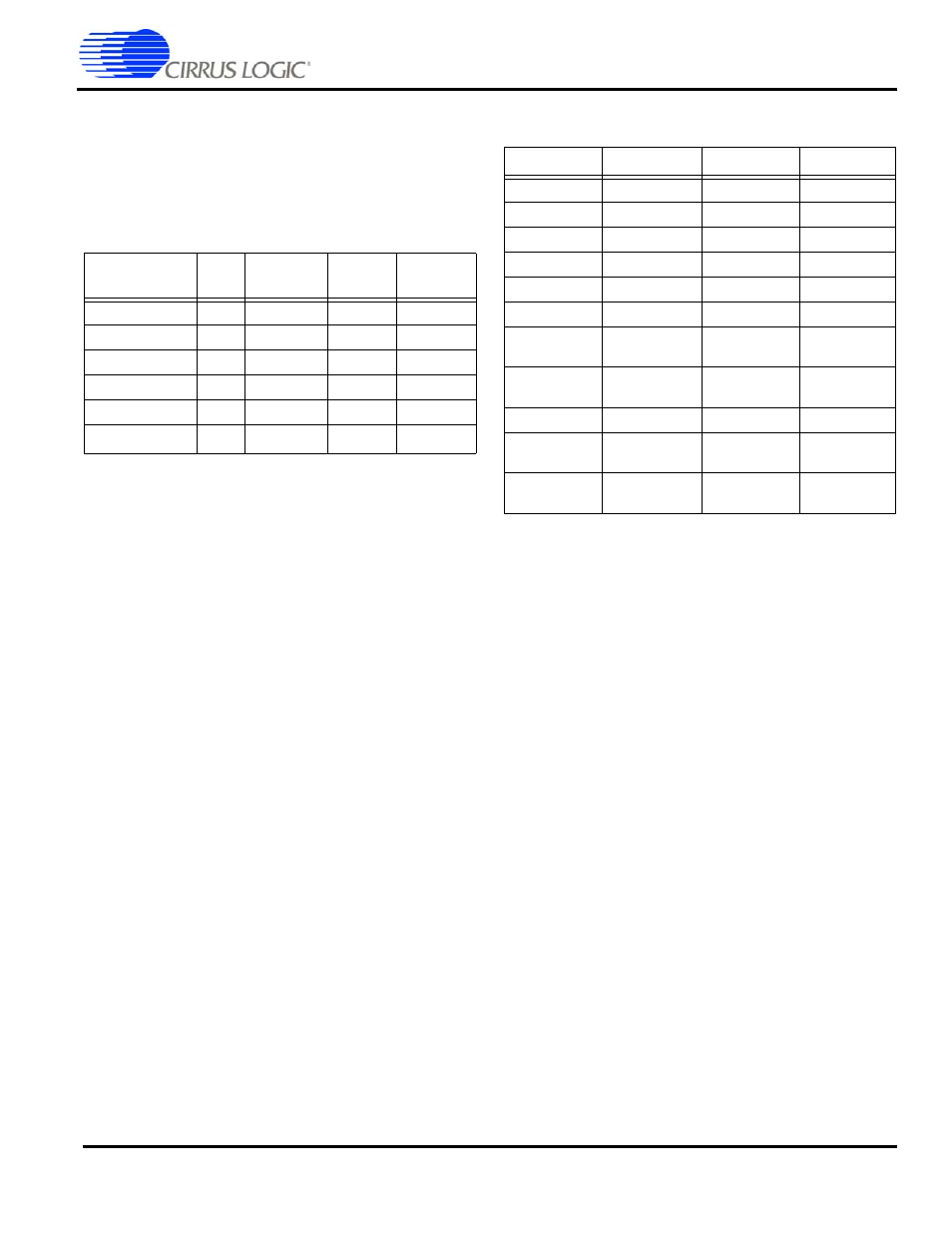
The following table shows the pin multiplexing of the MCP,
SSI2 and the CODEC. The selection between SSI2 and the
CODEC is controlled by the state of the SERSEL bit in
SYSCON2. The choice between the SSI2, CODEC, and the
MCP is controlled by the MCPSEL bit in SYSCON3 (see the
EP73xx User’s Manual for more information).
The following table shows the pins that have been multiplexed
in the EP7311.
Pin
Mnemonic
I/O
MCP
SSI2
CODEC
SSICLK
I/O
SIBCLK
SSICLK PCMCLK
SSITXDA
O
SIBDOUT
SSITXDA
PCMOUT
SSIRXDA
I
SIBDIN
SSIRXDA
PCMIN
SSITXFR
I/O
SIBSYNC
SSITXFR
PCMSYNC
SSIRXFR
I
p/u
SSIRXFR
p/u
BUZ
O
Table R. MCP/SSI2/CODEC Pin Multiplexing
Signal
Block
Signal
Block
nMOE
Static Memory
nSDCAS
SDRAM
nMWE
Static Memory
nSDWE
SDRAM
WRITE
Static Memory
nSDRAS
SDRAM
A[27:15]
Static Memory
DRA[0:12]
SDRAM
A[14:13]
Static Memory
DRA[13:14]
SDRAM
PD[7:6]
GPIO
SDQM[1:0]
SDRAM
RUN
System
Configuration
CLKEN
System
Configuration
nMEDCHG
Interrupt
Controller
nBROM
Boot ROM
select
PD[0]
GPIO
LEDFLSH
LED Flasher
PE[1:0]
GPIO
BOOTSEL[1:0]
System
Configuration
PE[2]
GPIO
CLKSEL
System
Configuration
Table S. Pin Multiplexing