Dc-to-dc converter interface (pwm), Timers, General purpose input/output (gpio) – Cirrus Logic EP7311 User Manual
Page 10: Hardware debug interface, Internal boot rom, Packaging, Led flasher
10
Copyright Cirrus Logic, Inc. 2011
(All Rights Reserved)
DS506F2
EP7311
High-Performance, Low-Power System on Chip
DC-to-DC converter interface (PWM)
•
Provides two 96 kHz clock outputs with programmable
duty ratio (from 1-in-16 to 15-in-16) that can be used to
drive a positive or negative DC to DC converter
Timers
•
Internal (RTC) timer
•
Two internal 16-bit programmable hardware count-down
timers
General Purpose Input/Output (GPIO)
•
Three 8-bit and one 3-bit GPIO ports
•
Supports scanning keyboard matrix
Note:
Pins are multiplexed. See
information.
Hardware debug Interface
•
Full JTAG boundary scan and Embedded ICE
support
LED Flasher
A dedicated LED flasher module can be used to generate a low
frequency signal on Port D pin 0 for the purpose of blinking an
LED without CPU intervention. The LED flasher feature is
ideal as a visual annunciator in battery powered applications,
such as a voice mail indicator on a portable phone or an
appointment reminder on a PDA.
•
Software adjustable flash period and duty cycle
•
Operates from 32 kHz RTC clock
•
Will continue to flash in IDLE and STANDBY states
•
4 mA drive current
Note:
Pins are multiplexed. See
for more
information.
Internal Boot ROM
The internal 128 byte Boot ROM facilitates download of saved
code to the on-board SRAM/FLASH.
Packaging
The EP7311 is available in a 208-pin LQFP package, 256-ball
PBGA package or a 204-ball TFBGA package.
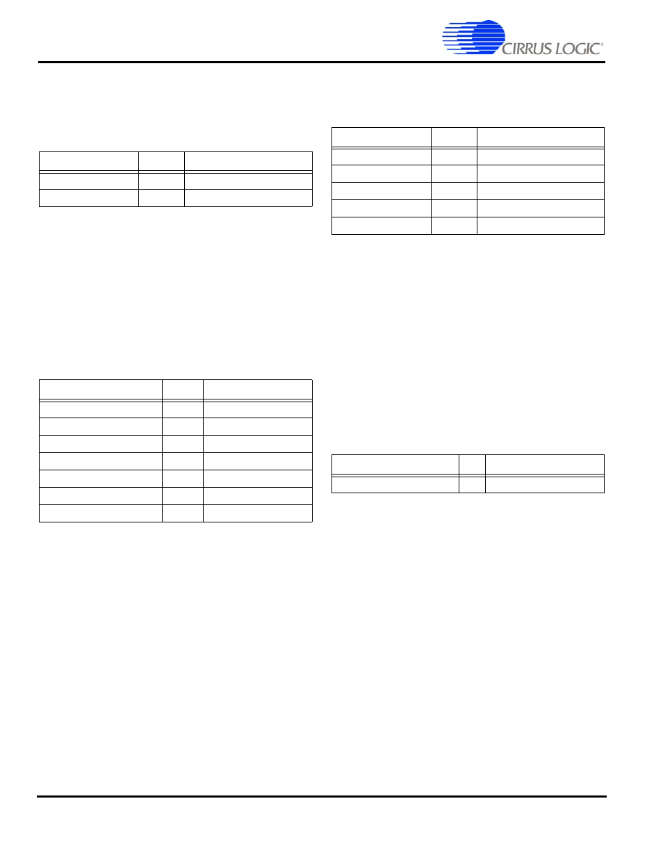
Pin Mnemonic
I/O
Pin Description
DRIVE[1:0]
I/O
PWM drive output
FB[1:0]
I
PWM feedback input
Table N. DC-to-DC Converter Interface Pin Assignments
Pin Mnemonic
I/O
Pin Description
PA[7:0]
I/O
GPIO port A
PB[7:0]
I/O
GPIO port B
PD[0]/LEDFLSH
(Note)
I/O
GPIO port D
PD[5:1]
I/O
GPIO port D
PD[7:6]/SDQM[1:0]
(Note)
I/O
GPIO port D
PE[1:0]/BOOTSEL[1:0] (Note)
I/O
GPIO port E
PE[2]/CLKSEL
(Note)
I/O
GPIO port E
Table O. General Purpose Input/Output Pin Assignments
Pin Mnemonic
I/O
Pin Description
TCLK
I
JTAG clock
TDI
I
JTAG data input
TDO
O
JTAG data output
nTRST
I
JTAG async reset input
TMS
I
JTAG mode select
Table P. Hardware Debug Interface Pin Assignments
Pin Mnemonic
I/O
Pin Description
PD[0]/LEDFLSH
(Note)
O
LED flasher driver
Table Q. LED Flasher Pin Assignments