Sdram load mode register cycle, Figure 3 – Cirrus Logic EP7311 User Manual
Page 17
DS506F2
Copyright Cirrus Logic, Inc. 2011
(All Rights Reserved)
17
EP7311
High-Performance, Low-Power System on Chip
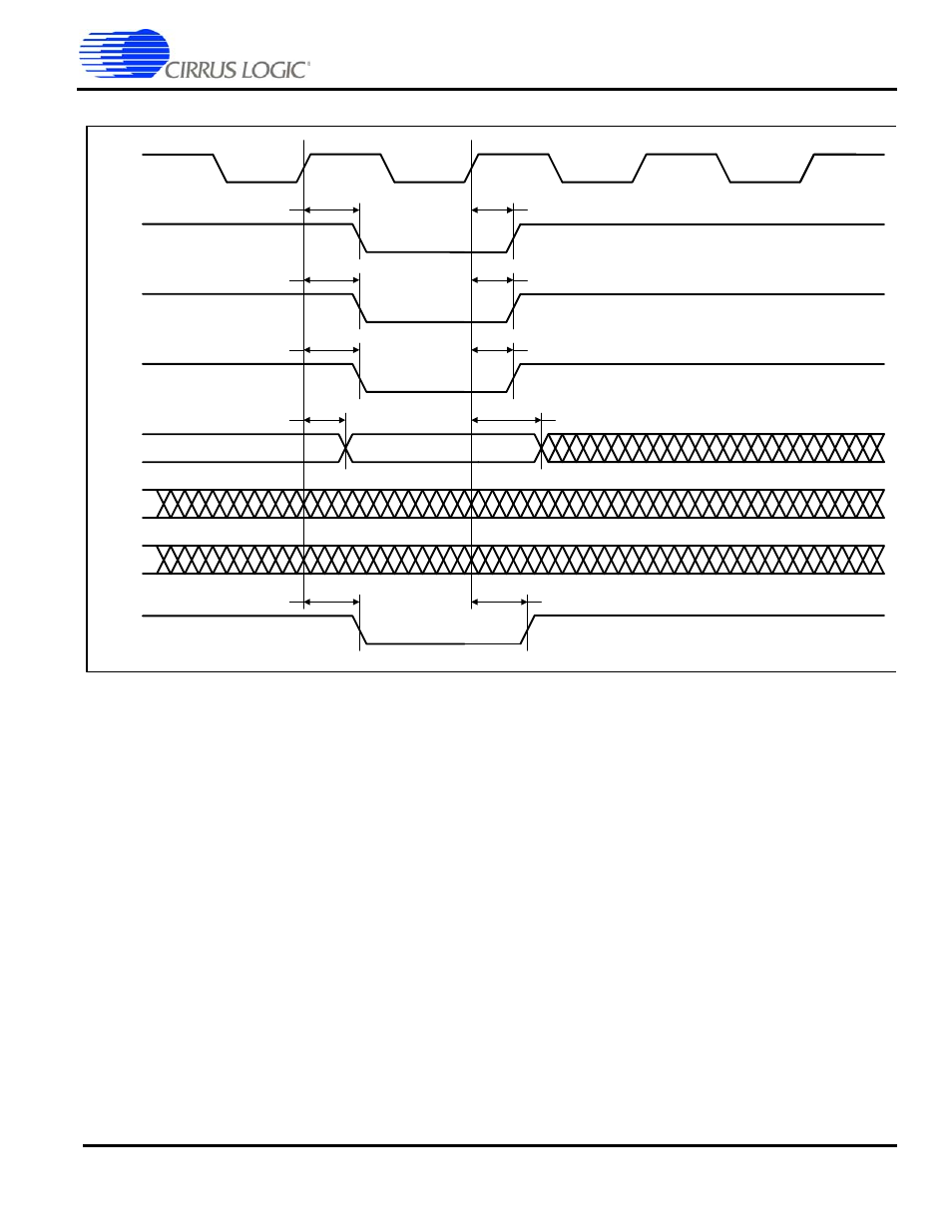
SDRAM Load Mode Register Cycle
Note:
1. Timings are shown with CAS latency = 2
2. The SDCLK signal may be phase shifted relative to the rest of the SDRAM control and data signals due to uneven loading.
Designers should take care to ensure that delays between SDRAM control and data signals are approximately equal
SDCLK
SDCS
SDRAS
SDCAS
ADDR
DATA
SDQM
SDMWE
t
CSa
t
RAa
t
CAa
t
MWa
t
ADv
t
ADx
t
RAd
t
CSd
t
CAd
t
MWd
Figure 3. SDRAM Load Mode Register Cycle Timing Measurement
See also other documents in the category Cirrus Logic Hardware:
- CobraNet (147 pages)
- CS4961xx (54 pages)
- CS150x (8 pages)
- CS1501 (16 pages)
- CS1601 (2 pages)
- CS1601 (16 pages)
- CS1610 (16 pages)
- CRD1610-8W (24 pages)
- CRD1611-8W (25 pages)
- CDB1610-8W (21 pages)
- CS1610A (18 pages)
- CDB1611-8W (21 pages)
- CDB1610A-8W (21 pages)
- CDB1611A-8W (21 pages)
- CRD1610A-8W (24 pages)
- CRD1611A-8W (25 pages)
- CS1615 (16 pages)
- AN403 (15 pages)
- AN401 (14 pages)
- AN400 (15 pages)
- AN375 (27 pages)
- AN376 (9 pages)
- CRD1615-8W (22 pages)
- CRD1616-8W (23 pages)
- AN402 (14 pages)
- AN404 (15 pages)
- CRD1615A-8W (21 pages)
- CS1615A (16 pages)
- CS1630 (56 pages)
- AN374 (35 pages)
- AN368 (80 pages)
- CRD1630-10W (24 pages)
- CRD1631-10W (25 pages)
- CS1680 (16 pages)
- AN405 (13 pages)
- AN379 (31 pages)
- CRD1680-7W (31 pages)
- AN335 (10 pages)
- AN334 (6 pages)
- AN312 (14 pages)
- AN Integrating CobraNet into Audio Products (16 pages)
- CobraNet Audio Routing Primer (9 pages)
- Bundle Assignments in CobraNet Systems (3 pages)
- CS2300-01 (3 pages)
- CS2000-CP (38 pages)