Cirrus Logic CS8415A User Manual
Cs8415a, 96 khz digital audio interface receiver, Features
Copyright
© Cirrus Logic, Inc. 2005
(All Rights Reserved)
96 kHz Digital Audio Interface Receiver
Features
!
Complete EIAJ CP1201, IEC-60958, AES3,
S/PDIF-compatible Receiver
!
+5.0 V Analog Supply (VA+)
!
+3.3 V or +5.0 V Digital Interface (VL+)
!
7:1 S/PDIF Input MUX
!
Flexible 3-wire Serial Digital Output Port
!
8-kHz to 96-kHz Sample Frequency Range
!
Low-jitter Clock Recovery
!
Pin and Microcontroller Read Access to
Channel Status and User Data
!
Microcontroller and Standalone Modes
!
Differential Cable Receiver
!
On-chip Channel Status and User Data Buffer
Memories
!
Auto-detection of Compressed Audio Input
Streams
!
Decodes CD Q Sub-Code
!
OMCK System Clock Mode
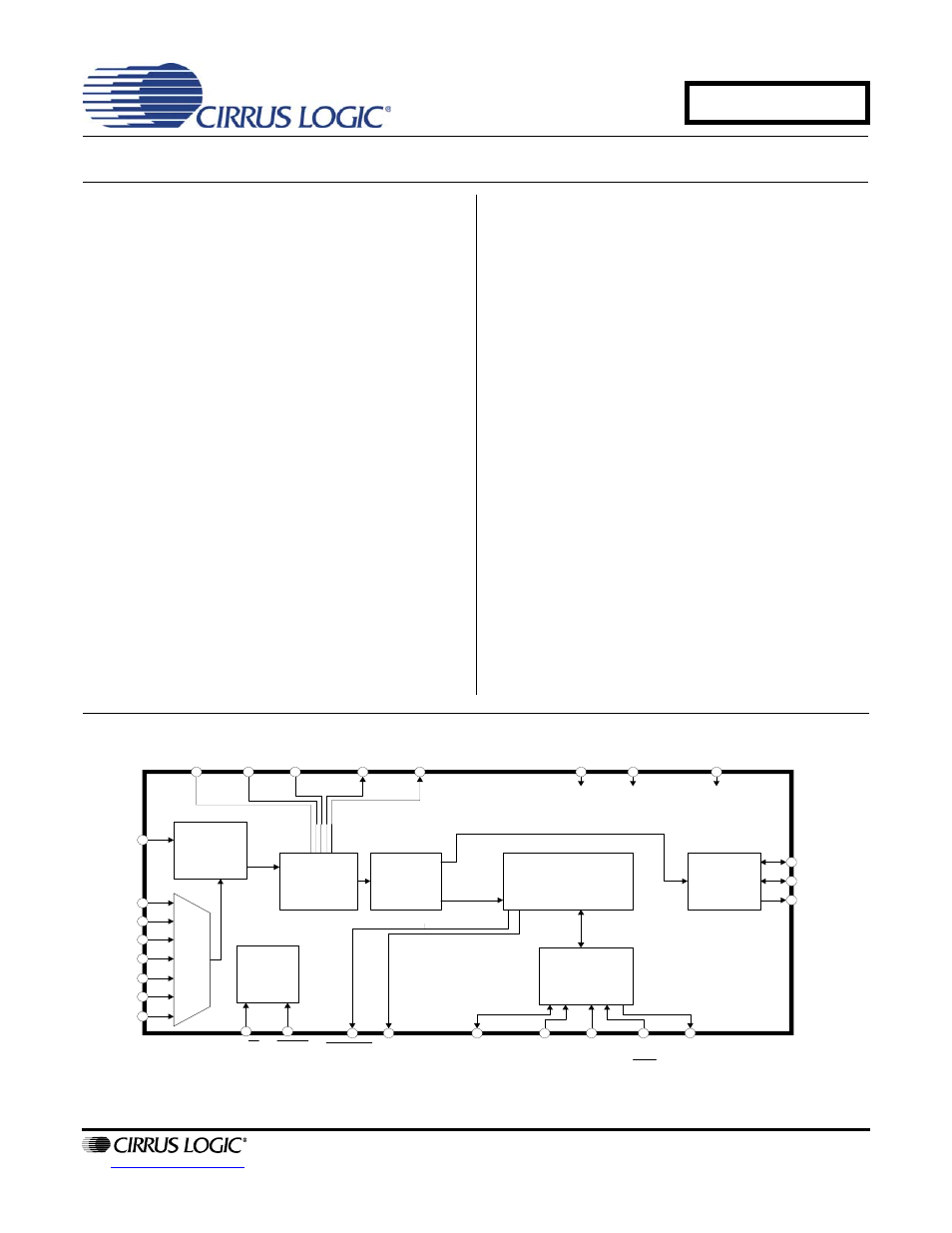
General Description
The CS8415A is a monolithic CMOS device which re-
ceives and decodes one of 7 channels of audio data
according to the IEC60958, S/PDIF, EIAJ CP1201, or
AES3. The CS8415A has a serial digital audio output
port and comprehensive control ability through a 4-wire
microcontroller port. Channel status and user data are
assembled in block-sized buffers, making read access
easy.
A low-jitter clock recovery mechanism yields a very
clean recovered clock from the incoming AES3 stream.
Stand-alone operation allows systems with no micro-
controller to operate the CS8415A with dedicated
output pins for channel status data.
The CS8415A is available in a 28-pin TSSOP and SOIC
package in both Commerical (-10 to +70°C) and Indus-
trial grades (-40 to +85° C). The CDB8415A Customer
Demonstration board is also available for device evalu-
ation and implementation suggestions. Please refer to
Target applications include A/V receivers, CD-R, DVD
receivers, multimedia speakers, digital mixing consoles,
effects processors, set-top boxes, and computer and
automotive audio systems.
Clock &
Data
Recovery
Misc.
Control
Serial
Audio
Output
Receiver
AES3
S/PDIF
Decoder
C & U bit
Data
Buffer
Control
Port &
Registers
RXN0
RXP6
OLRCK
OSCLK
SDOUT
RST
EMPH U
SDA/
CDOUT
SCL/
CCLK
AD1/
CDIN
AD0/
CS
INT
VA+ AGND FILT
RERR
VL + DGND
H/S
RMCK
RXP5
RXP4
RXP3
RXP2
RXP1
RXP0
7:1
MUX
OMCK
AUGUST '05
DS470F4
CS8415A
Document Outline
- 1. Characteristics and Specifications
- Specified Operating Conditions
- Absolute Maximum Ratings
- DC Electrical Characteristics
- Digital Input Characteristics
- Digital Interface Specifications
- Switching Characteristics
- Switching Characteristics - Serial Audio Ports
- Switching Characteristics - Control Port - SPI Mode
- Switching Characteristics - Control Port - I·C Mode
- 2. Typical Connection Diagram
- 3. General Description
- 4. Serial Audio output Port
- 5. AES3 Receiver
- 6. Control Port Description and Timing
- 7. Control Port Register Summary
- 8. Control Port Register Bit Definitions
- 8.1 Control 1 (01h)
- 8.2 Control 2 (02h)
- 8.3 Clock Source Control (04h)
- 8.4 Serial Audio Output Port Data Format (06h)
- 8.5 Interrupt 1 Status (07h) (Read Only)
- 8.6 Interrupt 2 Status (08h) (Read Only)
- 8.7 Interrupt 1 Mask (09h)
- 8.8 Interrupt 1 Mode MSB (0Ah) and Interrupt 1 Mode LSB (0Bh)
- 8.9 Interrupt 2 Mask (0Ch)
- 8.10 Interrupt 2 Mode MSB (0Dh) and Interrupt 2 Mode LSB (0Eh)
- 8.11 Receiver Channel Status (0Fh) (Read Only)
- 8.12 Receiver Error (10h) (Read Only)
- 8.13 Receiver Error Mask (11h)
- 8.14 Channel Status Data Buffer Control (12h)
- 8.15 User Data Buffer Control (13h)
- 8.16 Q-Channel Subcode Bytes 0 to 9 (14h - 1Dh) (Read Only)
- 8.17 OMCK/RMCK Ratio (1Eh) (Read Only)
- 8.18 C-bit or U-bit Data Buffer (20h - 37h)
- 8.19 CS8415A I.D. and Version Register (7Fh) (Read Only)
- 9. Pin Description - Software Mode
- 10. Hardware Mode
- 11. Pin Description - Hardware Mode
- 12. Applications
- 13. Appendix A: External AES3/SPDIF/IEC60958 Receiver Components
- 14. Appendix B: Channel Status and User Data Buffer Management
- 15. Appendix C: PLL Filter
- 16. Revision History