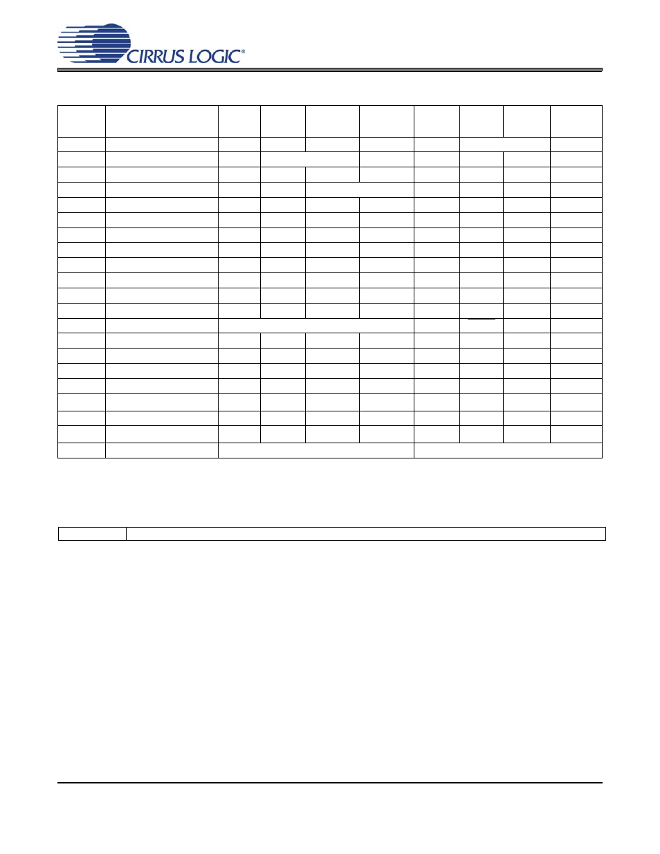
Control port register summary, Table 1. control register map summary, 1 memory address pointer (map) – Cirrus Logic CS8415A User Manual
Page 20

20
DS470F4
CS8415A
7. CONTROL PORT REGISTER SUMMARY
7.1
Memory Address Pointer (MAP)
INCR - Auto Increment Address Control Bit
Default = ‘0’
0 - Disabled
1 - Enabled
MAP6:MAP0 - Register address
Note:
Reserved registers must not be written to during normal operation. Some reserved registers are
used for test modes, which can completely alter the normal operation of the CS8415A.
Addr
(HEX)
Function
7
6
5
4
3
2
1
0
01
Control 1
SWCLK
0
MUTESAO
0
0
INT1
INT0
0
02
Control 2
0
HOLD1
HOLD0
RMCKF
MMR
MUX2
MUX1
MUX0
04
Clock Source Control
0
RUN
0
0
0
0
0
0
06
Serial Output Format
SOMS
SOSF
SORES1
SORES0
SOJUST
SODEL
SOSPOL
SOLRPOL
07
Interrupt 1 Status
0
OSLIP
0
0
0
DETC
0
RERR
08
Interrupt 2 Status
0
0
0
0
DETU
0
QCH
0
09
Interrupt 1 Mask
0
OSLIPM
0
0
0
DETCM
0
RERRM
0A
Interrupt 1 Mode (MSB)
0
OSLIP1
0
0
0
DETC1
0
RERR1
0B
Interrupt 1 Mode (LSB)
0
OSLIP0
0
0
0
DETC0
0
RERR0
0C
Interrupt 2 Mask
0
0
0
0
DETUM
0
QCHM
0
0D
Interrupt 2 Mode (MSB)
0
0
0
0
DETU1
0
QCH1
0
0E
Interrupt 2 Mode (LSB)
0
0
0
0
DETU0
0
QCH0
0
0F
Receiver CS Data
AUX3
AUX2
AUX1
AUX0
PRO
AUDIO
COPY
ORIG
10
Receiver Errors
0
QCRC
CCRC
UNLOCK
V
CONF
BIP
PAR
11
Receiver Error Mask
0
QCRCM
CCRCM
UNLOCKM
VM
CONFM
BIPM
PARM
12
CS Data Buffer Control
0
0
BSEL
CBMR
DETCI
0
CAM
CHS
13
U Data Buffer Control
0
0
0
0
0
0
DETUI
0
14-1D
Q sub-code Data
1E
OMCK/RMCK Ratio
ORR7
ORR6
ORR5
ORR4
ORR3
ORR2
ORR1
ORR0
20-37
C or U Data Buffer
7F
ID and Version
ID3
ID2
ID1
ID0
VER3
VER2
VER1
VER0
Table 1. Control Register Map Summary
7
6
5
4
3
2
1
0
INCR
MAP6
MAP5
MAP4
MAP3
MAP2
MAP1
MAP0
