Pin description - software mode – Cirrus Logic CS8415A User Manual
Page 30

30
DS470F4
CS8415A
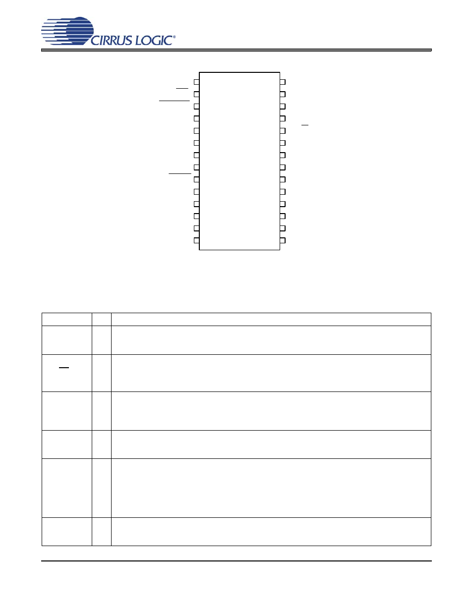
9. PIN DESCRIPTION - SOFTWARE MODE
Pin Name
#
Pin Description
SDA/CDOUT
1
Serial Control Data I/O (I²C) / Data Out (SPI) (Input/Output) - In I²C mode, SDA is the control I/O data
line. SDA is open drain and requires an external pull-up resistor to VL+. In SPI mode, CDOUT is the out-
put data from the control port interface on the CS8415A
AD0/CS
2
Address Bit 0 (I²C) / Control Port Chip Select (SPI) (Input) - A falling edge on this pin puts the
CS8415A into SPI control port mode. With no falling edge, the CS8415A defaults to I²C mode. In I²C
mode, AD0 is a chip address pin. In SPI mode, CS is used to enable the control port interface on the
CS8415A
EMPH
3
Pre-Emphasis (Output) - EMPH
is low when the incoming Channel Status data indicates 50/15 ms
pre-emphasis.
EMPH
is high when the Channel Status data indicates no pre-emphasis or indicates pre-
emphasis other than 50/15 ms. This is also a start-up option pin, and requires a 47 k
Ω resistor to either
VL+ or DGND, which determines the AD2 address bit for the control port in I²C mode
RXP0
RXN0
4
5
AES3/SPDIF Receiver Port (Input) - Differential line receiver inputs carrying AES3 data. RXP0 may be
used as a single-ended input as part of 7:1 S/PDIF Input MUX. If RXP0 is used in MUX, RXN0 must be
ac coupled to ground.
RXP1
RXP2 RXP3
RXP4 RXP5
RXP6
12
13
14
15
25
26
Additional AES3/SPDIF Receiver Port (Input) - Single-ended receiver inputs carrying AES3 or S/PDIF
digital data. These inputs, along with RXP0, comprise the 7:1 S/PDIF Input Multiplexer and select line
control is accessed using the MUX2:0 bits in the Control 2 register. Please note that any unused inputs
should be tied to ground. See Appendix A for recommended input circuits.
VA+
6
Positive Analog Power (Input) - Positive supply for the analog section. Nominally +5.0 V. This supply
should be as quiet as possible since noise on this pin will directly affect the jitter performance of the
recovered clock
SDA/CDOUT
AD0/CS
EMPH
RXP0
RXN0
VA+
AGND
FILT
RST
RMCK
RERR
RXP1
28
27
26
25
*24
*23
*22
*21
20
19
*18
*17
*16
15
1
2
3*+
4*
5*
6*
7*
8*
9*
10*
11*
12
13
14
SCL/CCLK
AD1/CDIN
H/S
V +
DGND
OMCK
U
INT
SDOUT
OLRCK
OSCLK
* Pins which remain the same function in all modes.
+ Pins which require a pull up or pull down resistor
to select the desired startup option.
RXP2
RXP3
RXP4
RXP6
RXP5
L
