Typical connection diagram – Cirrus Logic CS8415A User Manual
Page 11
DS470F4
11
CS8415A
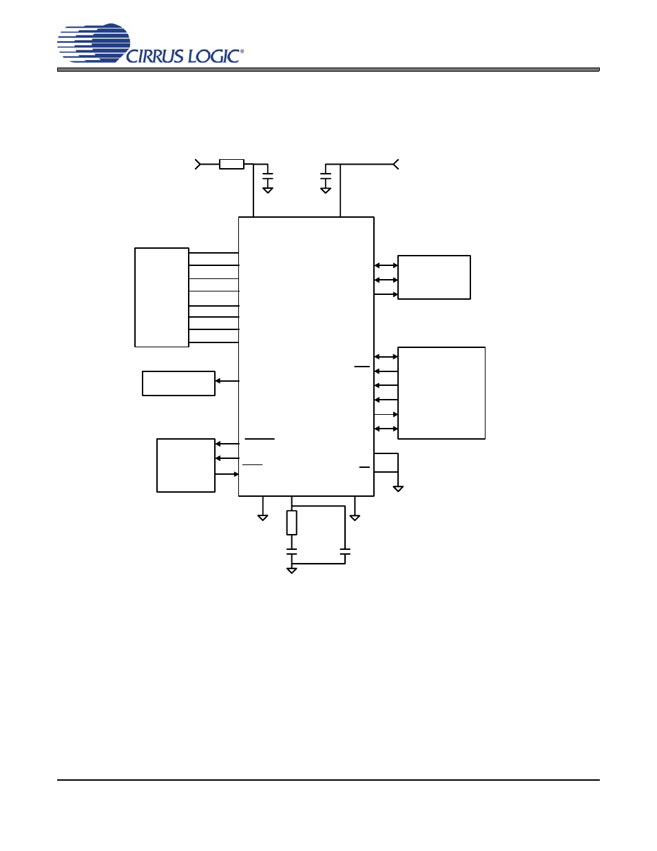
2. TYPICAL CONNECTION DIAGRAM
RXP0
RXN0
AES3/
SPDIF
Sources
Clock Control
RMCK
Hardware
Control
RST
RERR
EMPH
3-wire Serial
Audio Input
Device
OLRCK
OSCLK
SDOUT
SDA/CDOUT
AD0/CS
SCL/CCLK
AD1/CDIN
U
INT
VA+
V L+
Ferrite *
Bead
+5.0 V
Analog
Supply*
0.1 F
µ
0.1 F
µ
* A separate analog supply is only necessary in applications where RMCK is used
for a jitter sensitive task. For applications where RMCK is not used for a jitter
sensitive task, connect VA+ to VD+ via a ferrite bead. Keep the decoupling
capacitor between VA+ and AGND.
DGND
FILT
AGND
RFILT
CFILT
CRIP
H/S
DGND2
RXP1
RXP2
RXP3
RXP4
RXP5
RXP6
CS8415A
+3.3 V or +5.0 V
Digital Supply
* *
* * Please see section 5.1 "7:1 S/PDIF Input Multiplexer" and Appendix A for typical
input configurations and recommended input circuits.
A 2
D
/
Microcontroller
Figure 5. Recommended Connection Diagram for Software Mode
- CobraNet (147 pages)
- CS4961xx (54 pages)
- CS150x (8 pages)
- CS1501 (16 pages)
- CS1601 (2 pages)
- CS1601 (16 pages)
- CS1610 (16 pages)
- CRD1610-8W (24 pages)
- CRD1611-8W (25 pages)
- CDB1610-8W (21 pages)
- CS1610A (18 pages)
- CDB1611-8W (21 pages)
- CDB1610A-8W (21 pages)
- CDB1611A-8W (21 pages)
- CRD1610A-8W (24 pages)
- CRD1611A-8W (25 pages)
- CS1615 (16 pages)
- AN403 (15 pages)
- AN401 (14 pages)
- AN400 (15 pages)
- AN375 (27 pages)
- AN376 (9 pages)
- CRD1615-8W (22 pages)
- CRD1616-8W (23 pages)
- AN402 (14 pages)
- AN404 (15 pages)
- CRD1615A-8W (21 pages)
- CS1615A (16 pages)
- CS1630 (56 pages)
- AN374 (35 pages)
- AN368 (80 pages)
- CRD1630-10W (24 pages)
- CRD1631-10W (25 pages)
- CS1680 (16 pages)
- AN405 (13 pages)
- AN379 (31 pages)
- CRD1680-7W (31 pages)
- AN335 (10 pages)
- AN334 (6 pages)
- AN312 (14 pages)
- AN Integrating CobraNet into Audio Products (16 pages)
- CobraNet Audio Routing Primer (9 pages)
- Bundle Assignments in CobraNet Systems (3 pages)
- CS2300-01 (3 pages)
- CS2000-CP (38 pages)