Table 3. jitter attenuation selection – Cirrus Logic CS61880 User Manual
Page 12

CS61880
12
DS450PP3
WR/DS/SDI
84
J14
I
Write Enable/Data Strobe/Serial Data
Intel Parallel Host Mode - This pin, “WR”, functions as
a write enable.
Motorola Parallel Host Mode - This pin, “DS“, functions as
a data strobe input.
Serial Host Mode - This pin, “SDI”, functions as the serial
data input.
Hardware Mode - This pin is not used and should be con-
nected to ground.
RD/RW
85
J13
I
Read Enable/Read/Write
Intel Parallel Host Mode - This pin, “RD”, functions as a
read enable.
Motorola Parallel Host Mode - This pin, “R/W”, functions
as the read/write input signal.
Hardware Mode - This pin is not used and should be con-
nected to ground.
ALE/AS/SCLK
86
J12
I
Address Latch Enable/Address Strobe/Serial Clock
Intel Parallel Host Mode - This pin, “ALE”, functions as the
Address Latch Enable when configured for multiplexed ad-
dress/data operation.
Motorola Parallel Host Mode - This pin, “AS”, functions as
the active “low” address strobe when configured for multi-
plexed address/data operation.
Serial Host Mode - This pin, “SCLK”, is the serial clock
used for data I/O on SDI and SDO.
Hardware Mode - This pin is not used and should be con-
nected to ground.
CS/JASEL
87
J11
I
Chip Select Input/Jitter Attenuator Select
Host Mode - This active low input is used to enable ac-
cesses to the microprocessor interface in either serial or
parallel mode.
Hardware Mode - This pin controls the position of the Jitter
Attenuator.
SYMBOL
LQFP
FBGA
TYPE
DESCRIPTION
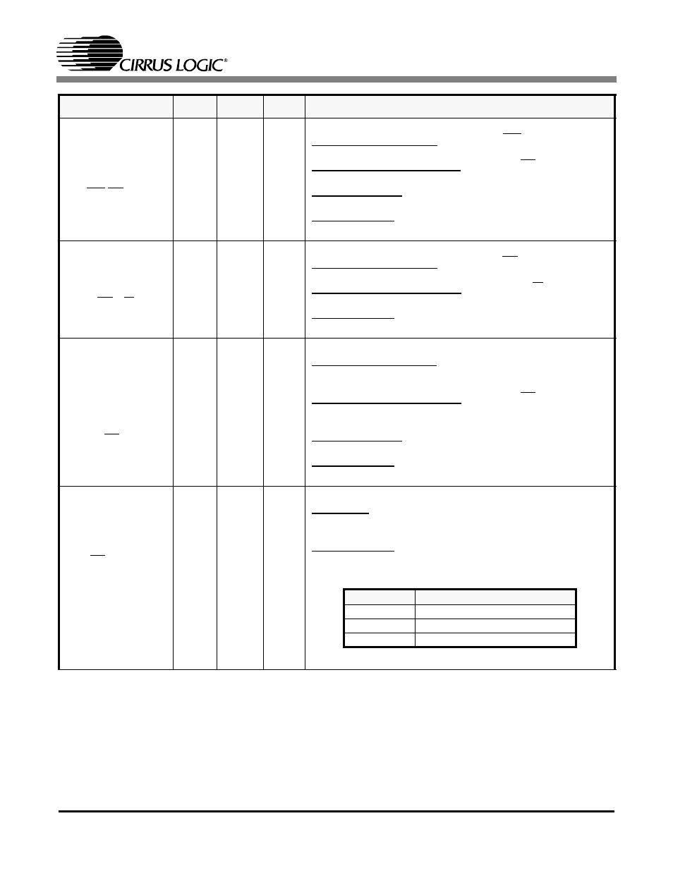
Table 3. Jitter Attenuation Selection
Pin State
Jitter Attenuation Position
LOW
Transmit Path
HIGH
Receive Path
OPEN
Disabled
