Pll and clock generation, 1 pin descriptions, 2 pll mode select – Cirrus Logic CS5378 User Manual
Page 22: 3 synchronous clocking, Pin descriptions, Pll mode select, Synchronous clocking, Figure 12. clock generation block diagram, Table 5. pll mode selections, Cs5378
CS5378
DS639F3
22
6. PLL AND CLOCK GENERATION
The CS5378 requires a 32.768 MHz master clock,
which can be supplied directly or from an internal
phase locked loop. This master clock is used to
generate an internal digital filter clock and an exter-
nal modulator clock.
The internal PLL will lock to standard clock or
Manchester encoded input signals. The input type
and input frequency are selected by the reset state
of the PLL mode select pins.
6.1 Pin Descriptions
CLK - Pin 17
Clock or PLL input, standard clock or Manchester.
GPIO[4:6]:PLL[0:2] - Pins 5, 6, 7
PLL mode select, latched immediately after reset.
Weak (~100 k
Ω) internal pull-ups default high, ex-
ternal 10 k
Ω pull-downs required to set low.
6.2 PLL Mode Select
The CS5378 PLL operational mode and frequency
are selected immediately after reset based on the
state of the PLL[0:2] pins. On the rising edge of the
reset signal, the digital high or low state of the
PLL[0:2] pins is latched and used to program the
clock input type and frequency.
A weak internal pull-up resistor (~100 k
Ω) will
hold the PLL mode select pins high by default. To
force the pin low on reset, an external 10 k
Ω pull-
down resistor should be connected. Once the pin
state is latched following reset, the GPIO[4:6] pins
function without affecting PLL operation.
6.3 Synchronous Clocking
To guarantee synchronous measurements through-
out a sensor network, a system clock should be dis-
tributed to arrive at all nodes in phase. The
distributed system clock can either be the full
32.768 MHz master clock, or the CS5378 PLL can
create a synchronous 32.768 MHz clock from a
slower clock. To ensure the generated clock re-
mains synchronous with the network, the CS5378
PLL uses a phase/frequency detector architecture.
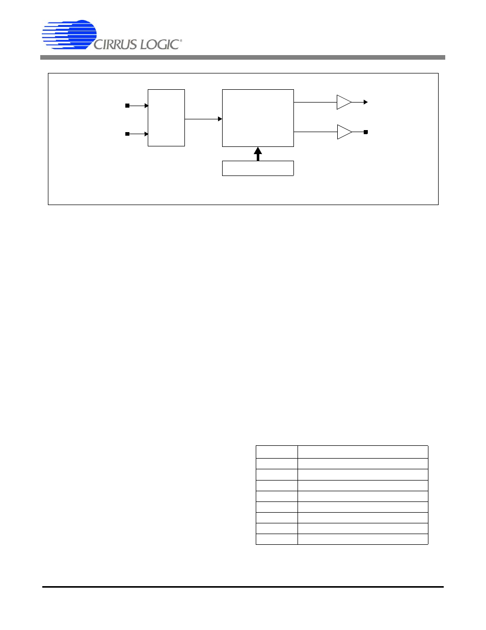
PLL
CLK
DSPCFG Register
MCLK
Internal
Clocks
Figure 12. Clock Generation Block Diagram
Clock Divider
Generator
and MCLK
Output
PLL[2:0]
32.768
MHz
PLL[2:0]
PLL Mode
111
32.768 MHz clock input (PLL bypass).
110
1.024 MHz clock input.
101
2.048 MHz clock input.
100
4.096 MHz clock input.
011
32.768 MHz clock input (PLL bypass).
010
1.024 MHz Manchester input.
001
2.048 MHz Manchester input.
000
4.096 MHz Manchester input.
Table 5. PLL Mode Selections