Power supplies, 1 pin descriptions, 2 bypass capacitors – Cirrus Logic CS5378 User Manual
Page 20: 3 power consumption, Pin descriptions, Bypass capacitors, Power consumption, Figure 10. power supply block diagram, Cs5378, 1 pin descriptions vddpad, gndpad - pins 9, 10
CS5378
DS639F3
20
4. POWER SUPPLIES
The CS5378 has three sets of power supply inputs.
One set supplies power to the I/O pins of the device
(VDDPAD), another supplies power to the logic
core (VDDCORE) and the third supplies power to
the PLL (VDDPLL). The I/O pin power supplies
determine the maximum input and output voltages
when interfacing to peripherals, the logic core pow-
er supply largely determines the power consump-
tion of the CS5378 and the PLL power supply
powers the internal PLL circuitry.
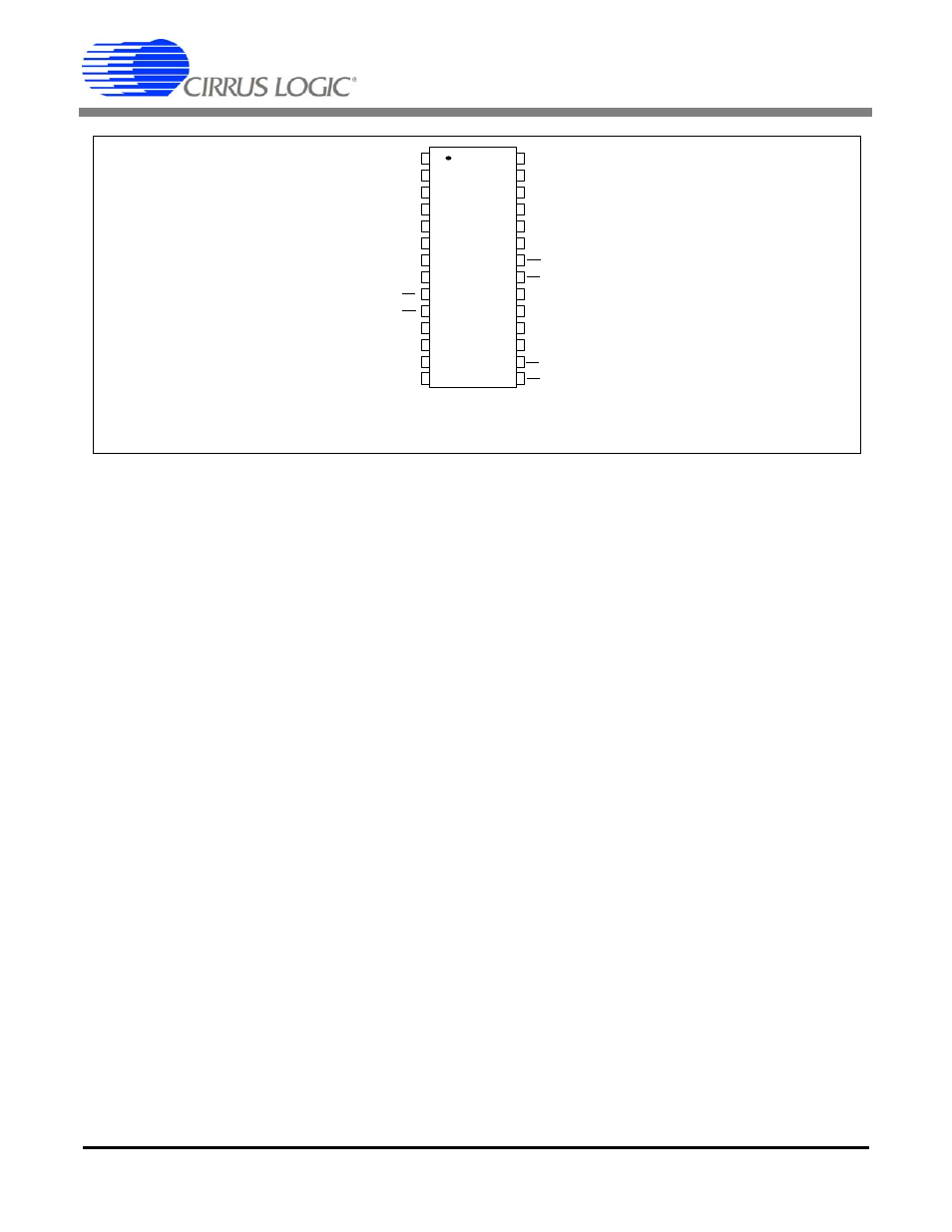
4.1 Pin Descriptions
VDDPAD, GNDPAD - Pins 9, 10
Sets the interface voltage to a microcontroller, sys-
tem telemetry, modulator, and test DAC. VDD-
PAD can be driven with voltages from 3.3 V to
5 V.
VDDPLL, GNDPLL - Pins 15, 16
Sets the operational voltage of the internal CS5378
PLL circuitry. Can be driven with voltages from
3.3 V to 5 V.
VDDCORE, GNDCORE - Pins 21, 22
Sets the operational voltage of the CS5378 logic
core. VDDCORE can be driven with voltages from
2.5 V to 5 V. A 2.5 V supply will minimize total
power consumption.
4.2 Bypass Capacitors
Each power supply pin should be bypassed with
parallel 1
μF and 0.01 μF caps, or by a single
0.1
μF cap, placed as close as possible to the
CS5378. Bypass capacitors should be ceramic
(X7R, C0G), tantalum, or other good quality di-
electric type.
4.3 Power Consumption
Power consumption of the CS5378 depends pri-
marily on the power supply voltage of the logic
core (VDDCORE) and the programmed digital fil-
ter clock rate. Digital filter clock rates are selected
based on the required output word rate as explained
in “Digital Filter Initialization” on page 38.
1
2
3
4
5
6
7
8
2 1
2 2
2 3
2 4
2 5
2 6
2 7
2 8
9
1 0
1 1
1 2
1 7
1 8
1 9
2 0
1 3
1 4
1 5
1 6
VDDPAD
GNDPAD
GNDCORE
VDDCORE
Figure 10. Power Supply Block Diagram
GNDPLL
VDDPLL