Cirrus Logic CS5378 User Manual
Cs5378 low-power single-channel decimation filter, Features, Description

Copyright
Cirrus Logic, Inc. 2010
(All Rights Reserved)
CS5378
Low-power Single-channel Decimation Filter
Features
Single-channel Digital Decimation Filter
Multiple On-chip FIR and IIR Coefficient Sets
Programmable Coefficients for Custom Filters
Synchronous Operation
Integrated PLL for Clock Generation
1.024 MHz, 2.048 MHz, or 4.096 MHz Input
Standard Clock or Manchester Input
Selectable Output Word Rate
4000, 2000, 1000, 500, 333, 250 SPS
200, 125, 100, 50, 40, 25, 20, 10, 5, 1 SPS
Digital Gain and Offset Corrections
Test DAC Bit-stream Generator
Digital Sine Wave Output
Time Break Controller, General-purpose I/O
Microcontroller or EEPROM Configuration
Small-footprint, 28-pin SSOP Package
Low Power Consumption
16 mW at 500 SPS OWR
Flexible Power Supplies
I/O Interface and PLL: 3.3 V or 5.0 V
Digital Logic Core: 2.5 V, 3.3 V or 5.0 V
Description
The CS5378 is a multi-function digital filter utilizing a low-
power signal processing architecture to achieve efficient
filtering for a delta-sigma-type modulator. By combining
the CS537 8 with a CS33 01A/02A di fferential a mplifier
and a CS5373A modulator + test DAC, a synchronous
high-resolution, self- testing, sin gle-channel m easure-
ment system can be designed quickly and easily.
Digital filter coefficients for the CS5378 FIR and IIR filters
are included on-chip for a simple setup, or they can be
programmed for custom ap plications. Selectable digital
filter decimation ratios produce output word rates from
4000 SPS to 1 SPS, resulting in measurement band-
widths ra nging fro m 16 00 Hz down to 400 mHz whe n
using the on-chip coefficient sets.
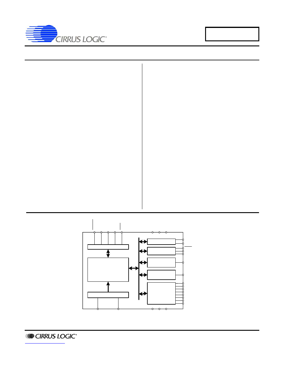
The CS5378 includes integrated peripherals to simplify
system d esign: a low- jitter PL L for standard clo ck or
Manchester inpu ts, offset and gain co rrections, a test
DAC bit stream generator, a tim e break controller, and
eight general-purpose I/O pins.
ORDERING INFORMATION
See
I
Serial Interface
Decimation and
Filtering Engine
Modulator Data Interface
Test Bit Stream
Controller
Reset, Synchronization
TBSDATA
Time Break Controller
GPIO
General Purpose I/O
SC
K
MO
S
I
VD
DP
AD
VD
DP
L
L
VD
DC
O
R
E
SYNC
MSYNC
TIMEB
GPIO5:PLL1
GPIO4:PLL0
GPIO3
GPIO2
GPIO1
GNDP
A
D
GNDC
ORE
GN
DP
L
L
MDATA
MF
LAG
GPIO0
GPIO6:PLL2
GPIO7:BOOT
DRD
Y
MIS
O
SS:
E
ECS
RESET
CLK
MCLK
PLL, Clock Generation
2&7 ‘10
DS639F3
Document Outline
- 1. General Description
- 2. Characteristics and Specifications
- 3. System Design with CS5378
- 4. Power Supplies
- 5. Reset Control
- 6. PLL and Clock Generation
- 7. Synchronization
- 8. Configuration By EEPROM
- 9. Configuration By Microcontroller
- 10. Modulator Interface
- 11. Digital Filter Initialization
- 12. SINC Filter
- 13. FIR Filter
- 14. IIR Filter
- 15. Gain and Offset Correction
- 16. Serial Data Interface
- 17. Test Bit Stream Generator
- 18. Time Break Controller
- 19. General Purpose I/O
- 20. Register Summary
- 21. Pin Description
- 22. Package Dimensions
- 23. Ordering Information
- 24. Environmental, Manufacturing, & Handling Information
- 25. Revision History
